Active device array substrate and display device

Inactive Publication Date: 2011-04-14
AU OPTRONICS CORP
View PDF13 Cites 38 Cited by
  • Summary
  • Abstract
  • Description
  • Claims
  • Application Information

AI Technical Summary

Benefits of technology

[0009]In view of the foregoing, the invention provides an active device array substrate,

Problems solved by technology

When the demands by the general public on the display quality and function continue to increase, the design of conductive lines, i.e. the circuit layout on an active device array substrate becomes more complicated.
Due to the demands on high image quality, the desi

Method used


Image

  • Active device array substrate and display device
  • Active device array substrate and display device
  • Active device array substrate and display device

Examples


Example

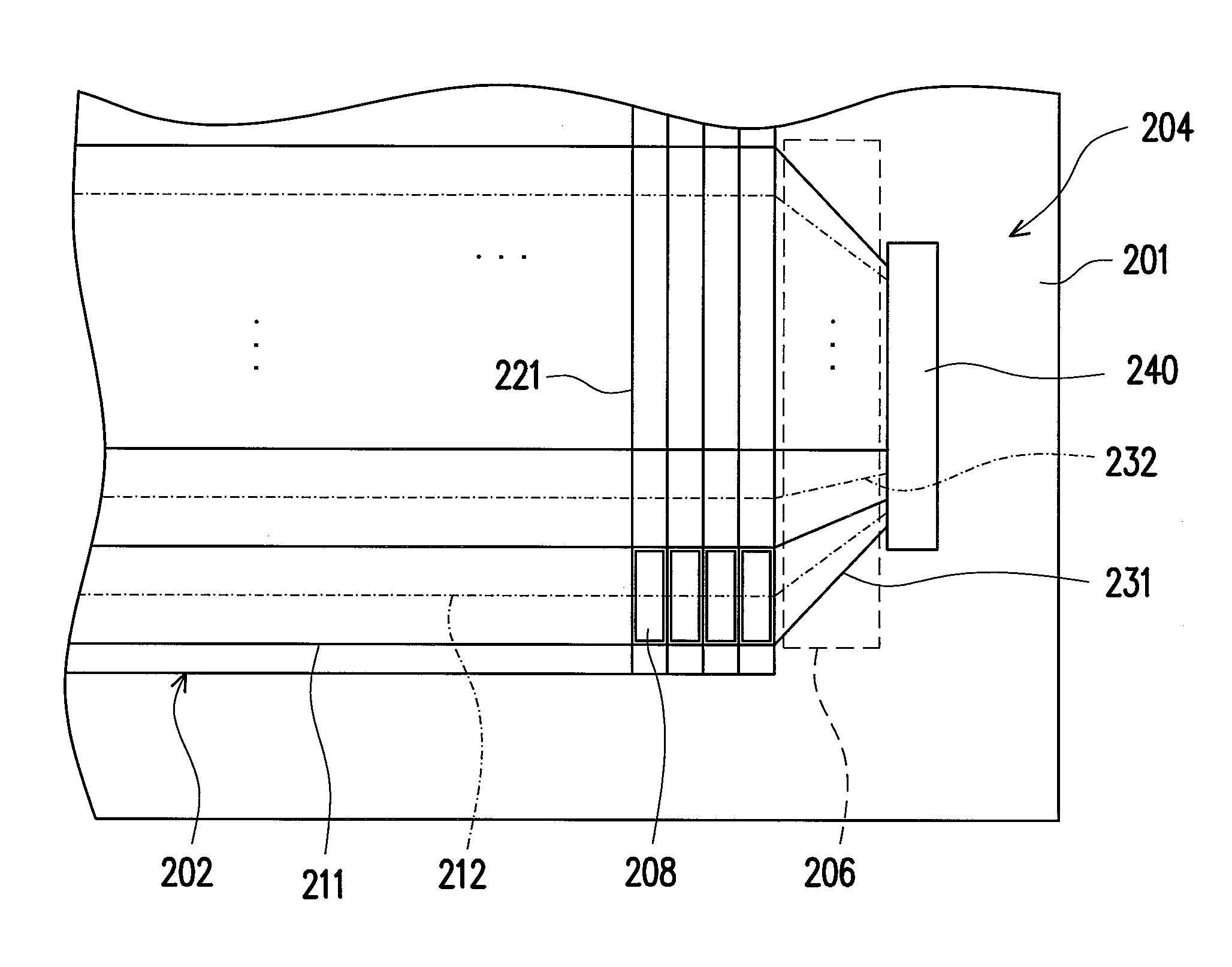
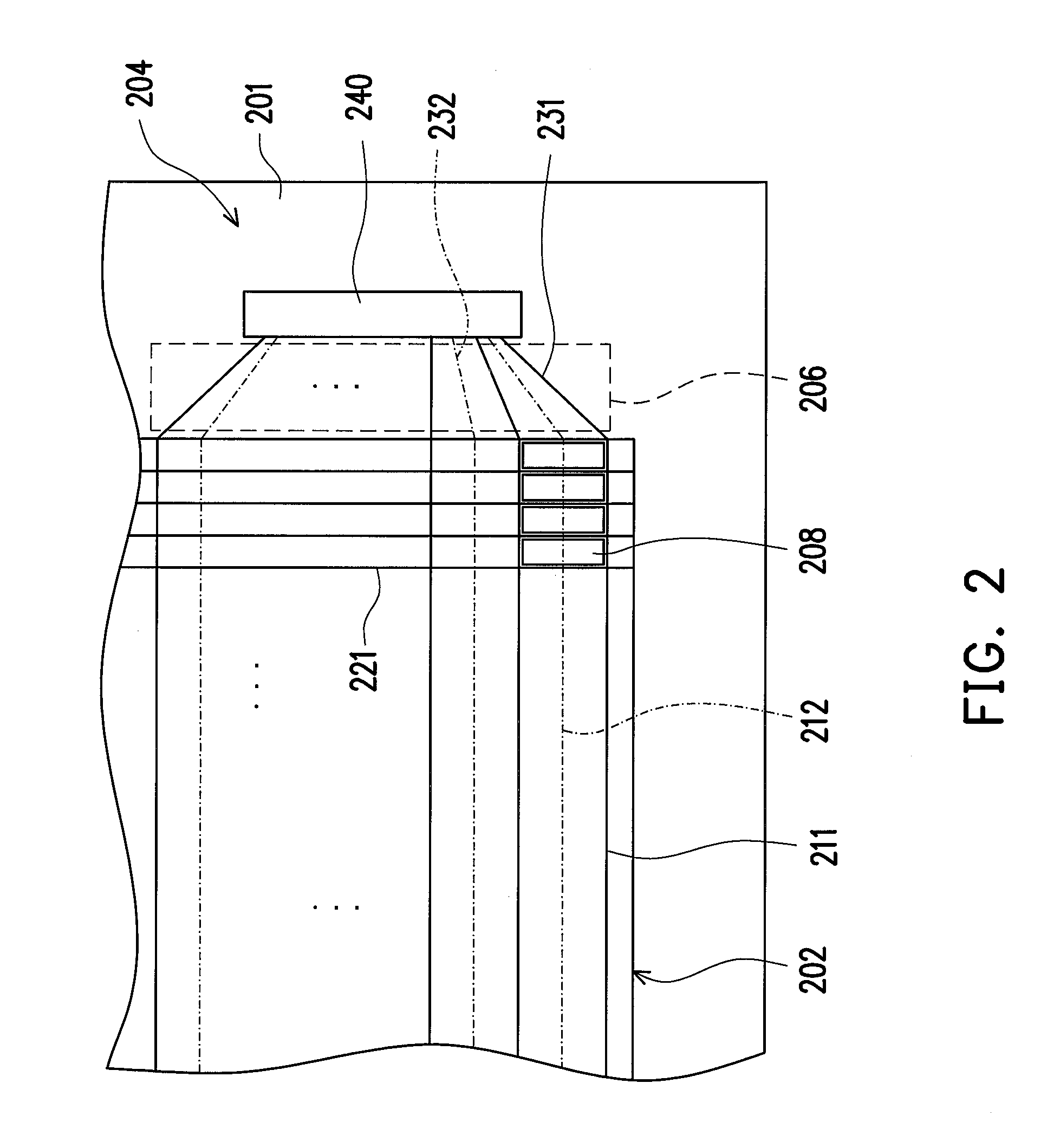
[0035]FIG. 2 is a partial top view diagram of an active device array substrate according to an embodiment of the invention. Referring to FIG. 2, the active device array substrate 200 includes a substrate 201, a plurality of scan lines 211, a plurality of control lines 212, a plurality of data lines 221, a plurality of pixel structures 208, a plurality of main transmission lines 231 and a plurality of sub transmission lines 232. The substrate 201 includes an active region 202 and a peripheral region 204, wherein the peripheral region 204 is configured at the periphery of the active region 202. The plurality of control lines 212 is disposed in the active region 202 of the substrate 201, parallel to the scan lines 211, wherein each scan line 211 is disposed next one control line 212. Simply speaking, the plurality control lines 212 and the plurality of scan lines 211 are disposed alternately.

[0036]The plurality of data lines 221 intersects with the plurality of scan lines 211 and the p...


PUM


Abstract

An active device array substrate including a substrate, scan lines, control lines, data lines, pixel structures, main transmission lines and sub transmission lines is provided. The substrate has an active area and a peripheral area. The scan lines and the control lines are disposed within the active area. The control lines are parallel to the scan lines and each control line is located between two of the scan lines. The main transmission lines located within the peripheral area are connected with the scan lines. The sub transmission lines located within the peripheral area are connected with the control lines. Each sub transmission line is located between two of the main transmission lines. Each main transmission line at least includes an impedance adjusting unit, and the impedance difference between each main transmission line and one of the adjacent sub transmission lines is larger than 3Ω.

Description

CROSS-REFERENCE TO RELATED APPLICATION[0001]This application claims the priority benefit of Taiwan application serial no. 98134645, filed on Oct. 13, 2009. The entirety of the above-mentioned patent application is hereby incorporated by reference herein and made a part of specification.BACKGROUND OF THE INVENTION[0002]1. Technical Field[0003]The invention relates to an active device array substrate and a display device. More particularly, the invention relates to an active device array substrate and a display device having uniform impedance and favorable display quality.[0004]2. Description of Related Art[0005]Generally speaking, a flat panel display device includes an active device array substrate, a color filter substrate and a back light module. When the demands by the general public on the display quality and function continue to increase, the design of conductive lines, i.e. the circuit layout on an active device array substrate becomes more complicated.[0006]FIG. 1 is a diagra...

Claims


Application Information

Patent Timeline
IPC IPC(8): G02F1/1345G09G3/20
CPCG02F1/13452G02F1/13338
Inventor FU, CHIEN-HAOHUANG, WEI-KAILIN, CHIA-CHIANGLIN, HSUEH-HUILEE, MING-CHIN
Owner AU OPTRONICS CORP
Why Eureka
Try Eureka