Method for decimation of images

a decimation method and image technology, applied in image data processing, instruments, printing, etc., can solve the problems of not giving accurate representation of micro-scale features, no suitable method for soldering mask patterning using laser, and unable to solve the problem of printed material accumulation, etc., to achieve accurate printing and limit the accumulation of printed materials

Inactive Publication Date: 2011-04-14
PALO ALTO RES CENT INC
View PDF4 Cites 29 Cited by
  • Summary
  • Abstract
  • Description
  • Claims
  • Application Information

AI Technical Summary

Problems solved by technology

Also, there is no suitable method for soldermask patterning using laser.
Photolithography is not an additive process, and so the problem of printed material accumulation may not arise even at high addressability.
However, this will not give an accurate representation of micro-scale features.
Failure to have good spot placement accuracy can result in patterning defects, which can reduce the yield and lead to inconsistent device performance.
When rasterization of the image is done at high addressability and then printed, there is a large three-dimensional accumulation of the material that is printed, which destroys the features that are obtained.

Method used

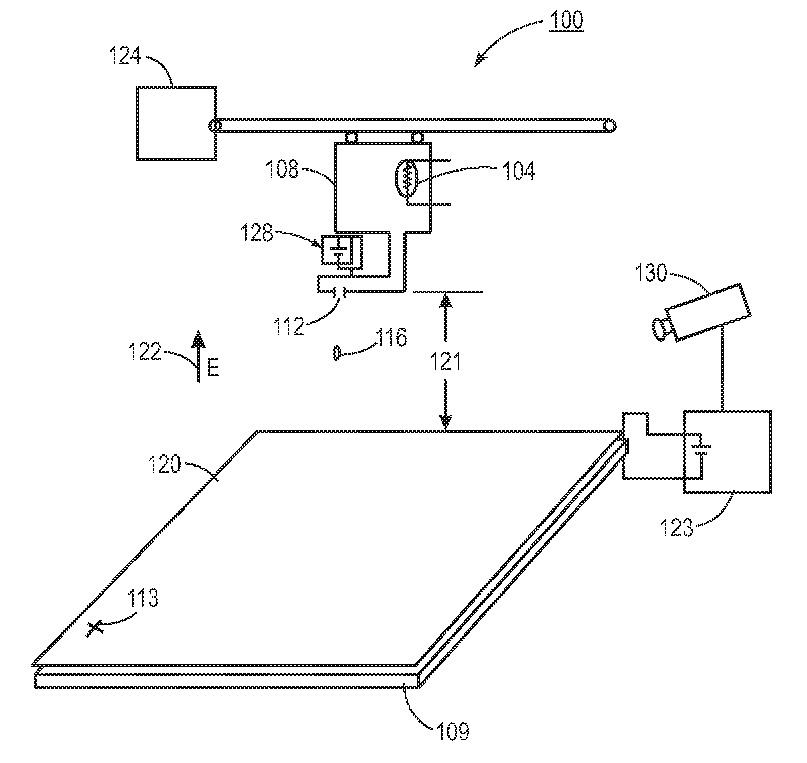
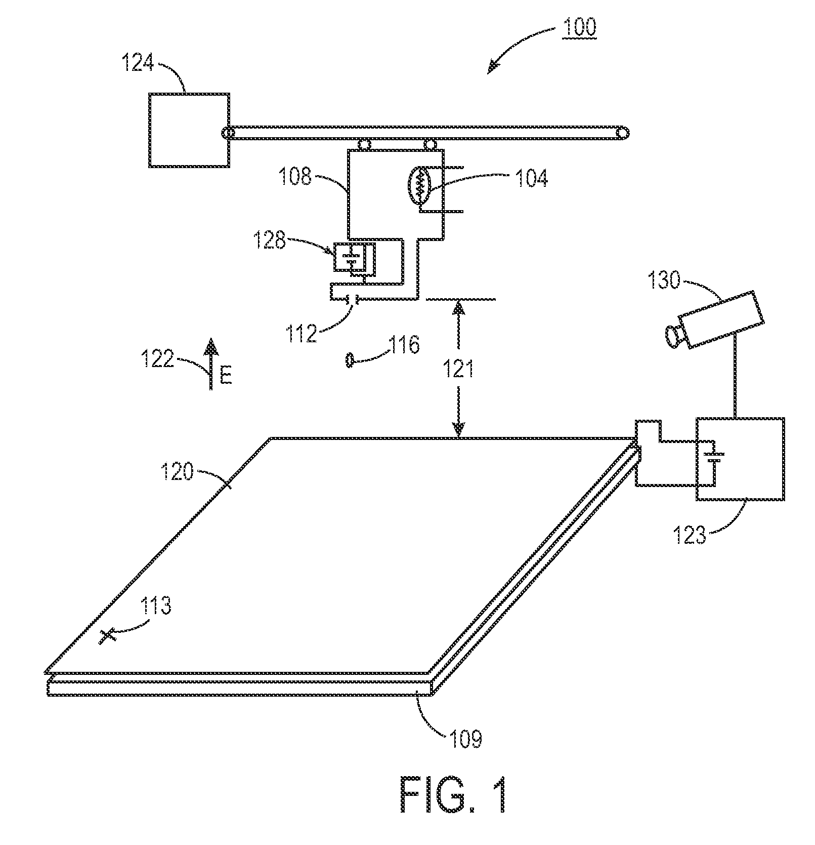

Image

  • Method for decimation of images
  • Method for decimation of images
  • Method for decimation of images

Examples


Embodiment Construction

[0051]Some portions of the detailed description that follows are presented in terms of algorithms and symbolic representations of operations on data bits performed by conventional computer components, including a central processing unit (CPU), memory storage devices for the CPU, and connected display devices. These algorithmic descriptions and representations are the means used by those skilled in the data processing arts to most effectively convey the substance of their work to others skilled in the art. An algorithm is generally perceived as a self-consistent sequence of steps leading to a desired result. The steps are those requiring physical manipulations of physical quantities. Usually, though not necessarily, these quantities take the form of electrical or magnetic signals capable of being stored, transferred, combined, compared, and otherwise manipulated. It has proven convenient at times, principally for reasons of common usage, to refer to these signals as bits, values, ele...


PUM


Abstract

In the case of printing at high addressability, where the cell size is smaller than the spot size, an image can be decimated in a manner that will limit the large accumulation of printed material. The proper decimation of the image will depend on the spot size, the physics of drop coalescence and the addressability during printing. A simple method of using concentric decimation is disclosed herein to enable this process.

Description

[0001]This is a divisional application of U.S. patent application Ser. No. 11 / 644,238, filed Dec. 22, 2006, which is hereby incorporated herein by reference in its entirety.BACKGROUND[0002]The exemplary embodiment relates generally to image processing systems and, more particularly, to a method of decimating images.[0003]A printed circuit board, or PCB, is a self-contained module of interconnected electronic components found in devices ranging from common beepers, or pagers, and radios to sophisticated radar and computer systems. The circuits are generally formed by a thin layer of conducting material deposited, or “printed,” on the surface of an insulating board known as the substrate. Individual electronic components are placed on the surface of the substrate and soldered to the interconnecting circuits. Contact fingers along one or more edges of the substrate act as connectors to other PCBs or to external electrical devices such as on-off switches. A printed circuit board may hav...

Claims


Application Information

Patent Timeline
Patent Type & Authority Applications(United States)
IPC IPC(8): G06F17/17
CPCH05K3/1241G06T3/4023B41J29/38
Inventor SRINIVASAN, UMAWHITE, STEPHEN DAVID
Owner PALO ALTO RES CENT INC
Why Eureka
Try Eureka