Semiconductor device

a technology of semiconductor devices and semiconductors, applied in semiconductor/solid-state device testing/measurement, testing circuits, instruments, etc., can solve problems such as difficulty in directly testing bump pads, and achieve the effect of being ready to test and reliabl

Active Publication Date: 2011-04-21
SAMSUNG ELECTRONICS CO LTD
View PDF5 Cites 32 Cited by
  • Summary
  • Abstract
  • Description
  • Claims
  • Application Information

AI Technical Summary

Benefits of technology

[0007]Exemplary embodiments provide a semiconductor device that can be readily and reliably tested.

Problems solved by technology

However, when the μ-bump technique is applied, it can be difficult to directly probe a bump pad during a wafer test of a semiconductor device because the size of the bump pad on which a μ-bump is disposed is very small.

Method used


Image

  • Semiconductor device
  • Semiconductor device
  • Semiconductor device

Examples


Embodiment Construction

[0053]Various exemplary embodiments will now be described more fully with reference to the accompanying drawings in which exemplary embodiments are shown. The present inventive concept may, however, be embodied in many different forms and should not be construed as limited to the exemplary embodiments set forth herein.

[0054]It will be understood that when an element is referred to as being “connected” or “coupled” to another element, it can be directly connected or coupled to the other element or intervening elements may be present.

[0055]Exemplary embodiments relate to a semiconductor device and a test system of the semiconductor device. Like numbers refer to like elements throughout the description of the figures.

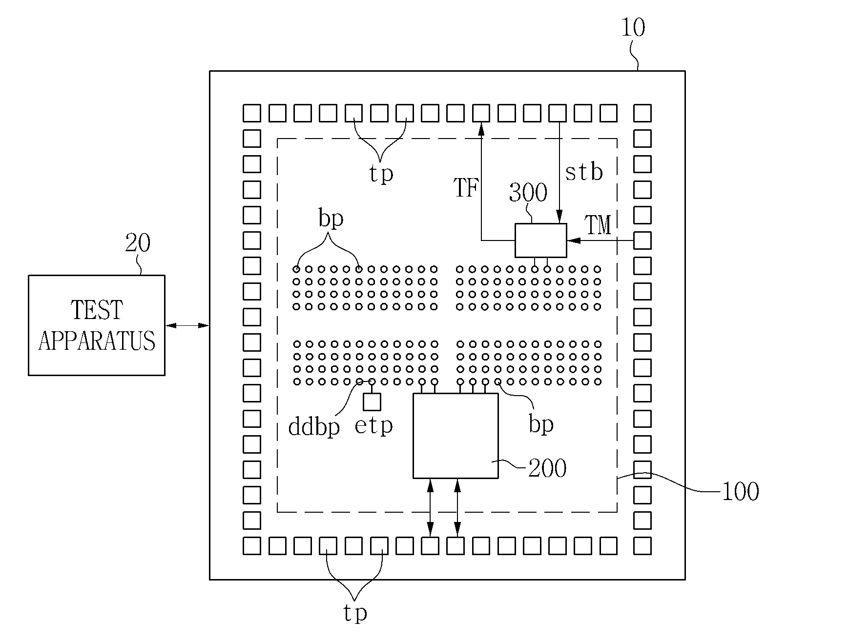
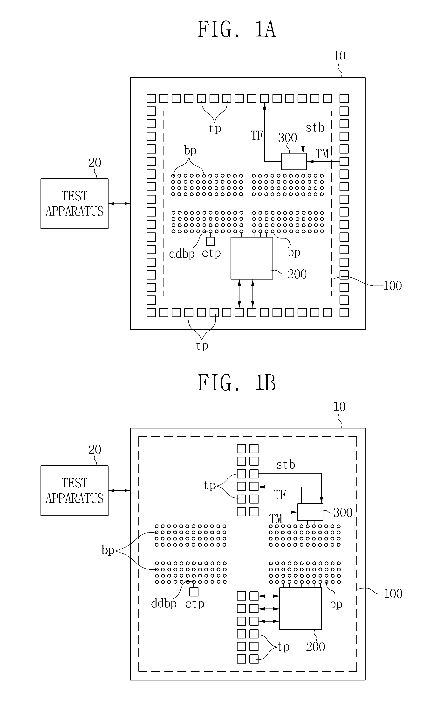
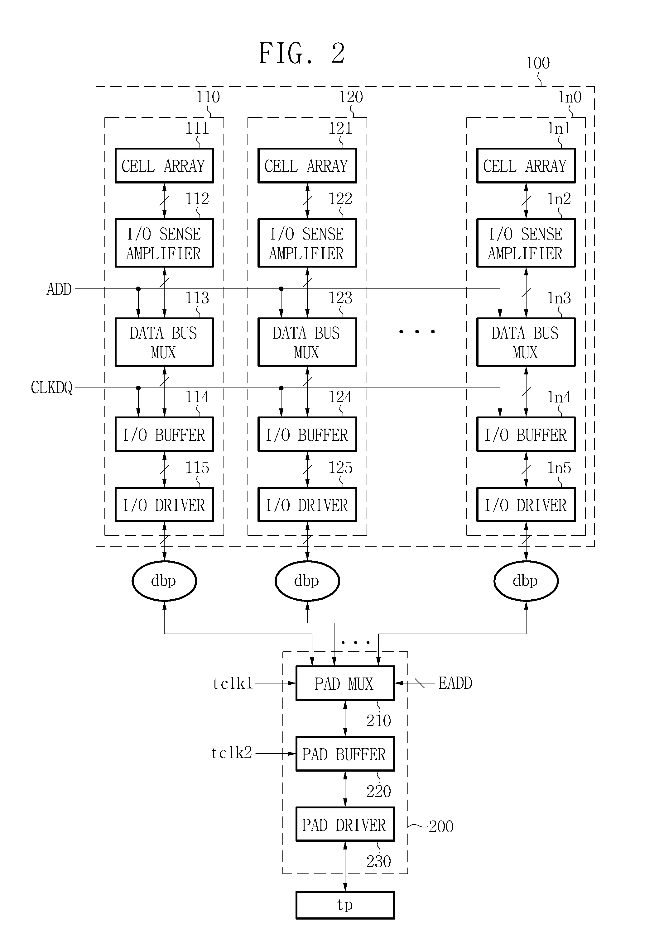
[0056]FIGS. 1A and 1B are block diagrams of a semiconductor device having a bump according to exemplary embodiments. A semiconductor device 10 includes an internal circuit 100, a test data selector 200, a sampling circuit 300, a plurality of bump pads bp, and a plurality o...


PUM


Abstract

A semiconductor device is provided. The semiconductor device applies data applied through a bump pad on which a bump is mounted through a test pad to a test apparatus such that the reliability of the test can be improved. The amount of test pads is significantly reduced by allowing data output through bump pads to be selectively applied to a test pad. Data and signals applied from test pads are synchronized with each other and applied to bump pads during a test operation such that the reliability of the test can be improved without the need of an additional test chip.

Description

CROSS-REFERENCE TO RELATED APPLICATIONS[0001]This application claims under 35 U.S.C. §119 priority to and the benefit of Korean Patent Applications No. 10-2009-0098489, filed on Oct. 16, 2009 and No. 10-2010-0066439, filed on Jul. 9, 2010, the entire content of which is incorporated by reference herein.BACKGROUND[0002]1. Technical Field[0003]The present disclosure relates to semiconductor devices and semiconductor device test systems, and more particularly, to a semiconductor device capable of improving the reliability of a test.[0004]2. Discussion of Related Art[0005]As semiconductor devices increase in capacity and become more highly integrated, the amount of data that is simultaneously input and output is increasing. For this reason, the amount of input / output (I / O) pins that can be simultaneously accessed needs to increase to improve the performance of semiconductor devices. To meet this need, μ-bump technique has been developed as new packaging technology.[0006]However, when th...

Claims


Application Information

Patent Timeline
Patent Type & Authority Applications(United States)
IPC IPC(8): G01R31/14H03L7/00
CPCG01R31/31726G01R31/2884
Inventor OH, CHI-SUNGLEE, DONG-HYUKLEE, HO-CHEOLRYU, JANG-WOOLEE, JUNG-BAE
Owner SAMSUNG ELECTRONICS CO LTD
Why Eureka
Try Eureka