Charge pump utilizing external clock signal
- Summary
- Abstract
- Description
- Claims
- Application Information
AI Technical Summary
Problems solved by technology
Method used
Image

Examples
Embodiment Construction
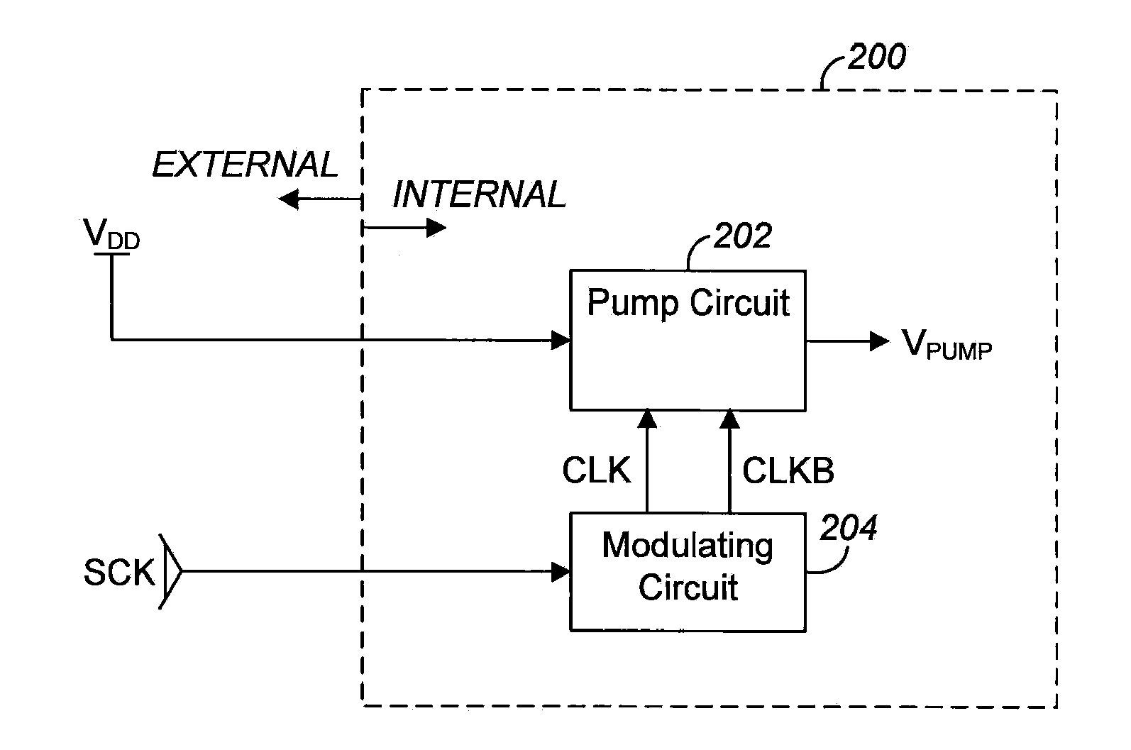
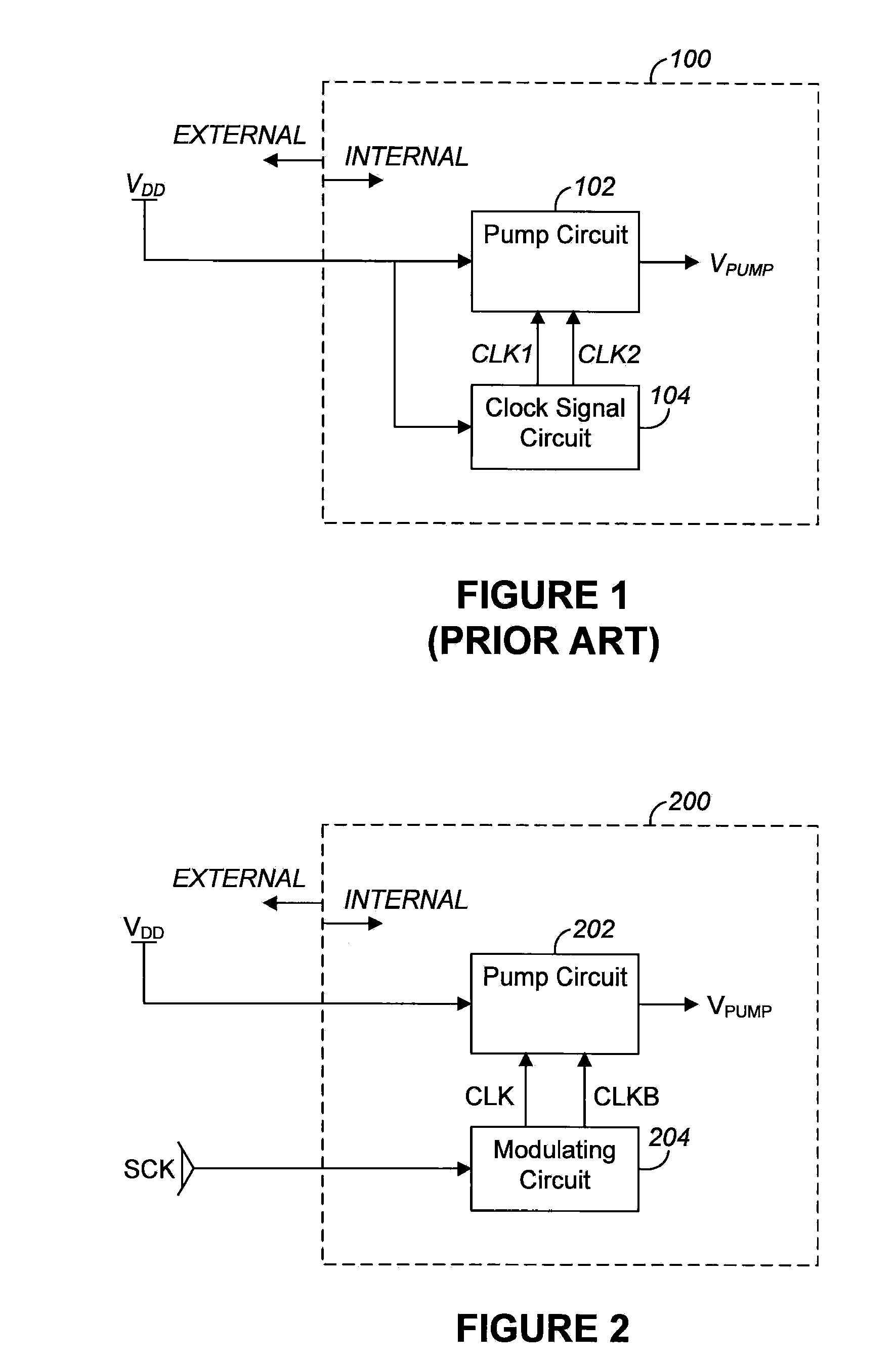
[0019]FIG. 2 shows a block diagram of an integrated circuit 200 in accordance with one embodiment can include a pump circuit 202 and a modulating circuit 204.
[0020]The modulating circuit 204 can be configured such that it receives a system clock signal SCK from a source that is external to the integrated circuit 200. The modulating circuit 204 can be configured such that the system clock signal SCK is selectively modulated and output as clock signals CLK and CLKB.
[0021]The pump circuit 202 can be configured such that it receives the clock signals CLK and CLKB and a supply voltage VDD. The pump circuit 202 can be configured such that the supply voltage VDD and clock signals CLK and CLKB are used to generate a pumping voltage VPUMP. The pump circuit 202 can be configured such that the pumping voltage VPUMP has a voltage level that is greater than that of the supply voltage VDD. The supply voltage VDD can be provided from a source that is external to the integrated circuit 200 as shown...
PUM
 Abstract
Description
Claims
Application Information
 - R&D Engineer
- R&D Manager
- IP Professional
- Industry Leading Data Capabilities
- Powerful AI technology
- Patent DNA Extraction
Browse by: Latest US Patents, China's latest patents, Technical Efficacy Thesaurus, Application Domain, Technology Topic.
© 2024 PatSnap. All rights reserved.Legal|Privacy policy|Modern Slavery Act Transparency Statement|Sitemap