Touch sensing display device with in-cell touch panel

a display device and touch panel technology, applied in the field of can solve the problems of low stability and reliability of in-cell touch sensing display devices, touch sensing signals applied to touch sensing elements are susceptible to interference, and common electrode layers may exist between touch sensing elements and touch sensing elements,

Inactive Publication Date: 2011-05-19
INNOLUX CORP
View PDF3 Cites 95 Cited by
  • Summary
  • Abstract
  • Description
  • Claims
  • Application Information

AI Technical Summary

Problems solved by technology

However, parasitic capacitors may exist between the common electrode layer and the touch sensing elements.
The parasitic capacitors may cause the touch sensing signals applied to the touch sensing elements to be susceptible to interference due to a variation of the AC common voltage signal.
Accordingly, the in-cell touch sensing display device has low stability and reliability.

Method used


Image

  • Touch sensing display device with in-cell touch panel
  • Touch sensing display device with in-cell touch panel
  • Touch sensing display device with in-cell touch panel

Examples


first embodiment

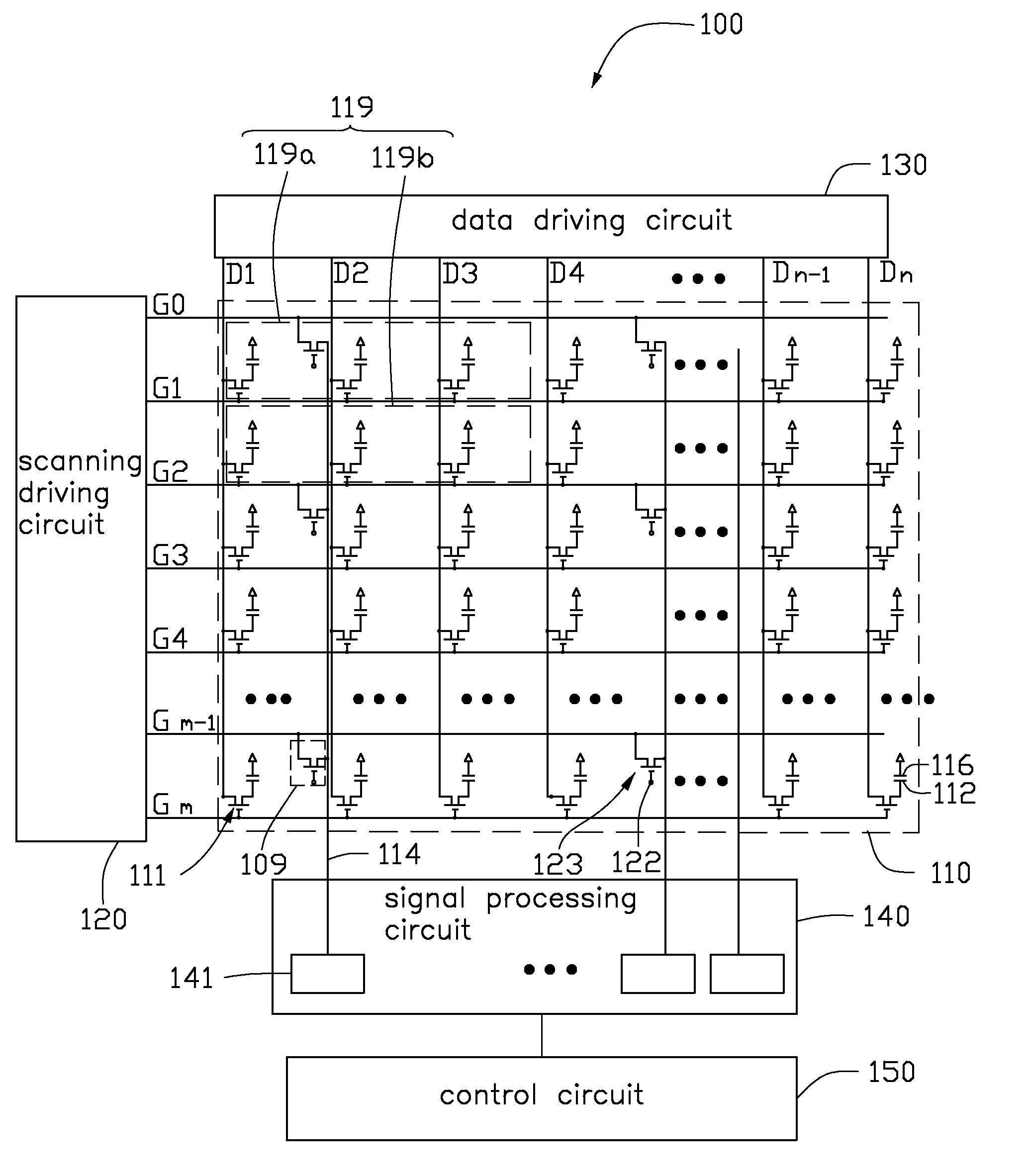
[0027]FIG. 1 schematically illustrates a partial circuit diagram of a touch sensing display device according to the present disclosure. The touch sensing display device 100 includes a touch panel 110, a scanning driving circuit 120, a data driving circuit 130, a signal processing circuit 140, and a control circuit 150.

[0028]The touch panel 110 can be a LCD panel with touch sensing elements built therein. The touch panel 110 may include a total m+1 parallel scanning lines G0˜Gm, a total n parallel data lines D1˜Dn, and a total m×n pixel units Pij arranged as a matrix distribution (where i, j respectively represent the ith row and the jth column of the pixel matrix, and 1≦i≦m, 1≦j≦n). In particular, the scanning lines G0˜Gm may be perpendicular to the data lines D1˜Dn, and the pixel units Pij are defined by intersection of the scanning lines G0˜Gm and the data lines D1˜Dn.

[0029]Each pixel unit Pij includes a thin film transistor (TFT) 111 and a pixel electrode 112. A gate electrode of...

second embodiment

[0043]Referring to FIG. 5, a partial circuit diagram of a touch sensing display device according to the present disclosure is shown. The touch sensing display device 200 is similar to the above-described touch sensing display device 100, differing in that: a touch sensing element 209 is disposed in a pixel unit of a second touch display sub-unit 219b, and the touch sensing element 209 is electrically coupled to the scanning line Gi (i denotes an odd number).

[0044]Referring to FIG. 6, waveforms of driving signals of the touch sensing display device of FIG. 5 is shown. In operation, the controllable switch of the processing module 241 is switched on when the corresponding scanning line Gi coupled to the touch sensing element 209 is provided with the scanning signal and the common electrode layer 216 is provided with a common voltage signal with a negative polarity. Accordingly, the processing module 241 can only read and process the touch sensing signal transmitted through the touch s...

third embodiment

[0045]Referring to FIG. 7, a partial circuit diagram of a touch sensing display device according to the present disclosure is shown. The touch sensing display device 300 is similar to the above-described touch sensing display device 100, differing in that each touch display unit 319 includes p×q pixel units (where p=3, q=1 in one embodiment), and a touch sensing element 309 is disposed in a selected pixel unit therein. The touch sensing element 309 is electrically coupled to a corresponding scanning line G0-Gm, and is also electrically coupled to a processing module 341 of a signal processing circuit 340 via a corresponding touch sensing line 314.

[0046]Referring to FIG. 8, waveforms of driving signals of the touch sensing display device of FIG. 7 is shown. In operation, during the Nth frame, when the scanning line Gi−1 is provided with the scanning signal, the common electrode layer 316 is provided with a common voltage signal with a positive polarity and the processing module 341 c...


PUM


Abstract

A touch sensing display device includes a touch panel and a signal processing circuit. The touch panel includes a plurality of pixel units, and the pixel units constitute a plurality of touch display units each comprising a touch sensing element. The touch sensing element is electrically coupled to a corresponding scanning line and electrically coupled to the signal processing circuit via a touch sensing line. A common voltage signal with a first polarity and an inversed second polarity is provided to the pixel unit. When the scanning line electrically coupled to the touch sensing element is provided with a scanning signal and the common voltage signal with the first polarity, a touch sensing signal generated by the touch sensing element is outputted to the signal processing circuit to enable the signal process circuit to generate a touch position indication signal.

Description

BACKGROUND[0001]1. Technical Field[0002]The present disclosure relates to touch sensing display devices, and more particularly to a touch sensing display device having a in-cell touch panel.[0003]2. Description of Related Art[0004]Touch sensing display devices, for example, in-cell type touch sensing display devices, are widely used in the electronic devices, such as mobile phones, game consoles, personal digital assistants (PDAs), and the like.[0005]An existing in-cell touch sensing display device usually includes a liquid crystal display (LCD) panel with touch sensing elements built inside the LCD panel cells. A user can operate the touch sensing display device by performing a touch operation onto the LCD panel, and thereby applying a touch sensing signal to the touch sensing elements.[0006]In particular, the LCD panel may further include a common electrode layer. In order to protect the liquid crystal molecules from decay or damage, an alternating circuit (AC) common voltage sign...

Claims


Application Information

Patent Timeline
Patent Type & Authority Applications(United States)
IPC IPC(8): G06F3/041
CPCG06F3/044G06F3/0412G06F3/0443G06F3/047
Inventor SHIH, PO-SHENG
Owner INNOLUX CORP
Why Eureka
Try Eureka