Semiconductor device

a technology of semiconductors and devices, applied in the direction of electric controllers, instruments, ignition automatic control, etc., can solve the problems of deterioration over time of batteries and lack of electric power occurring with discharge, and the problem of ensuring the safety of users, etc., to achieve the effect of stabilizing communication, and reducing the risk of electrical failur

Inactive Publication Date: 2008-03-06
SEMICON ENERGY LAB CO LTD
View PDF39 Cites 104 Cited by
  • Summary
  • Abstract
  • Description
  • Claims
  • Application Information

AI Technical Summary

Benefits of technology

[0023]One aspect of the semiconductor device of the present invention is that it includes a storage means that can be charged up. As a result, deterioration over time of a battery and lack of electric power occurring with discharge, as occurs in the conventional art, can be prevented. The storage means is not connected to a wiring of a charger, but the storage means can be charged up using electric power of electromagnetic waves received from an external source. Because of this, operations for checking the remaining battery capacity and for changing a battery, as for a battery of active RFID, become needless. Additionally, because electric power for driving the sem

Problems solved by technology

Meanwhile, in passive RFID like that shown in FIG. 20, because power for driving is produced using electric power of electromagnetic waves from an external source, securing electric power for transmission of information long distances is difficult and realizing stable comm

Method used


Image

  • Semiconductor device
  • Semiconductor device
  • Semiconductor device

Examples


embodiment mode 1

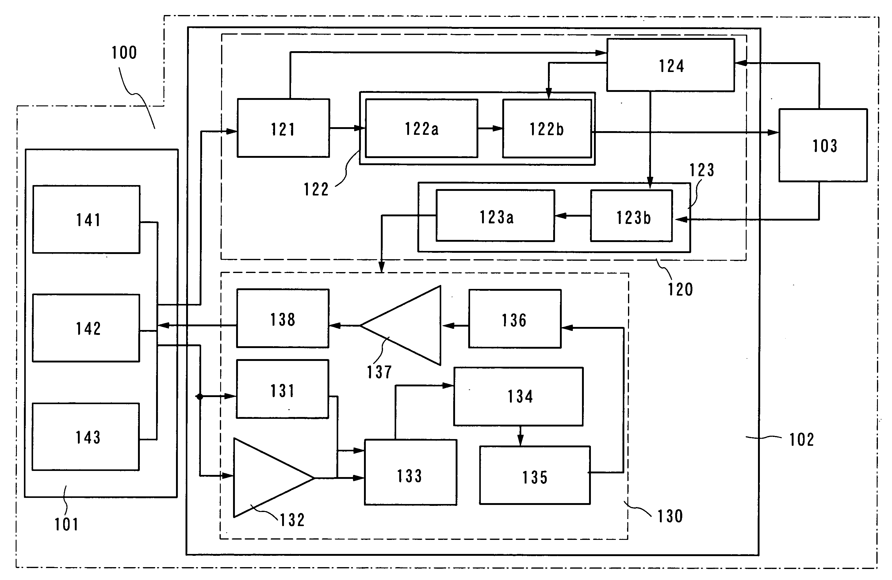
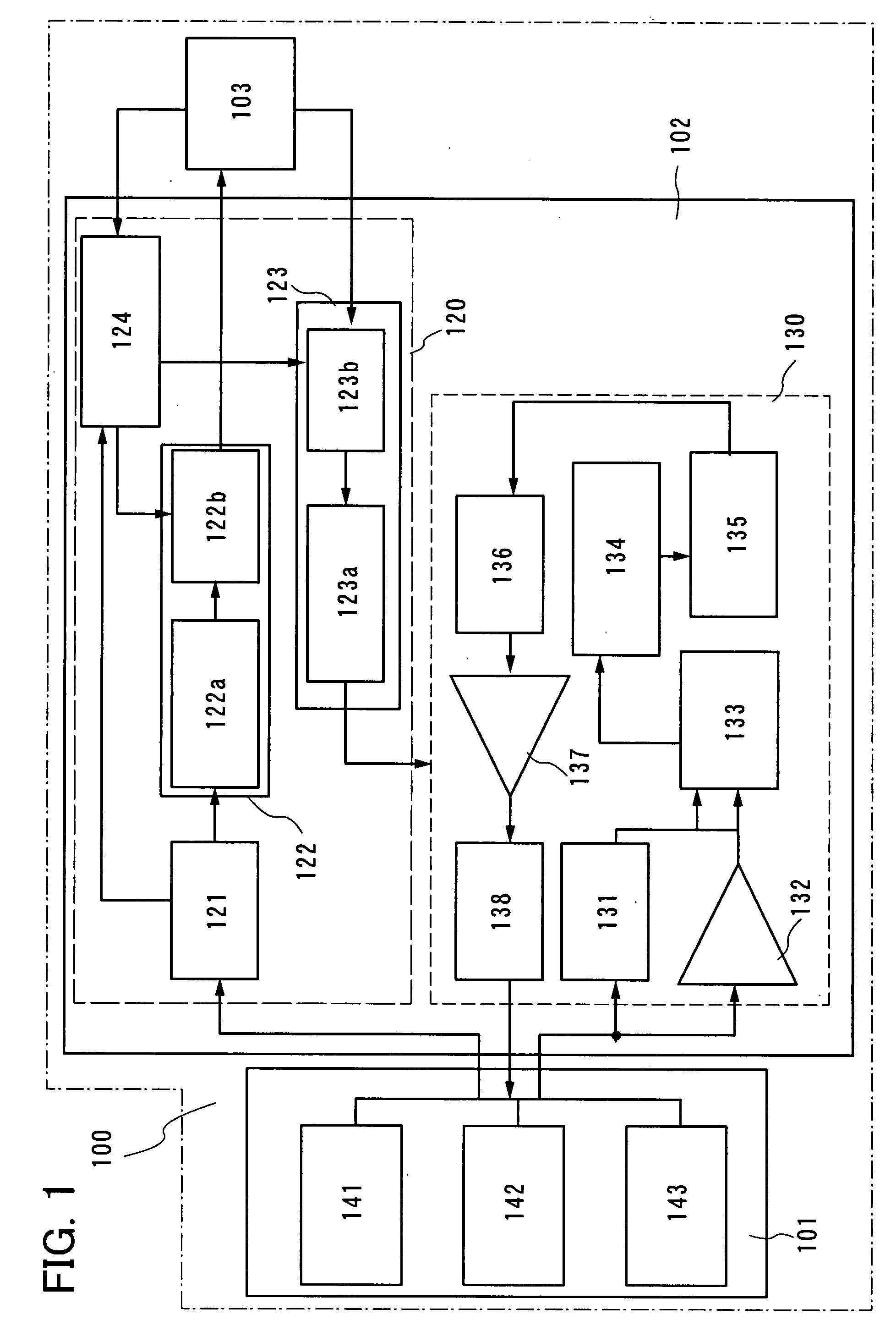
[0047]First, a structure of a semiconductor device related to Embodiment Mode 1 of the present invention will be described briefly. The semiconductor device includes an antenna circuit, a signal processing circuit for processing signals received by the antenna circuit, and a storage means for storing power produced by the signal processing circuit.

[0048]The antenna circuit is a circuit that receives and transmits signals. RFID of the present invention has a plurality of antenna portions, and each of the plurality of antenna portions receives signals at a frequency different from that of the others. In addition, an antenna terminal of the plurality of antenna portions is common. That is to say, in an antenna circuit, the plurality of antenna portions is connected to a signal processing section, which is to be described later, through a common antenna terminal.

[0049]The signal processing circuit includes a power section and a logic section. The power section generates a direct current...

embodiment mode 2

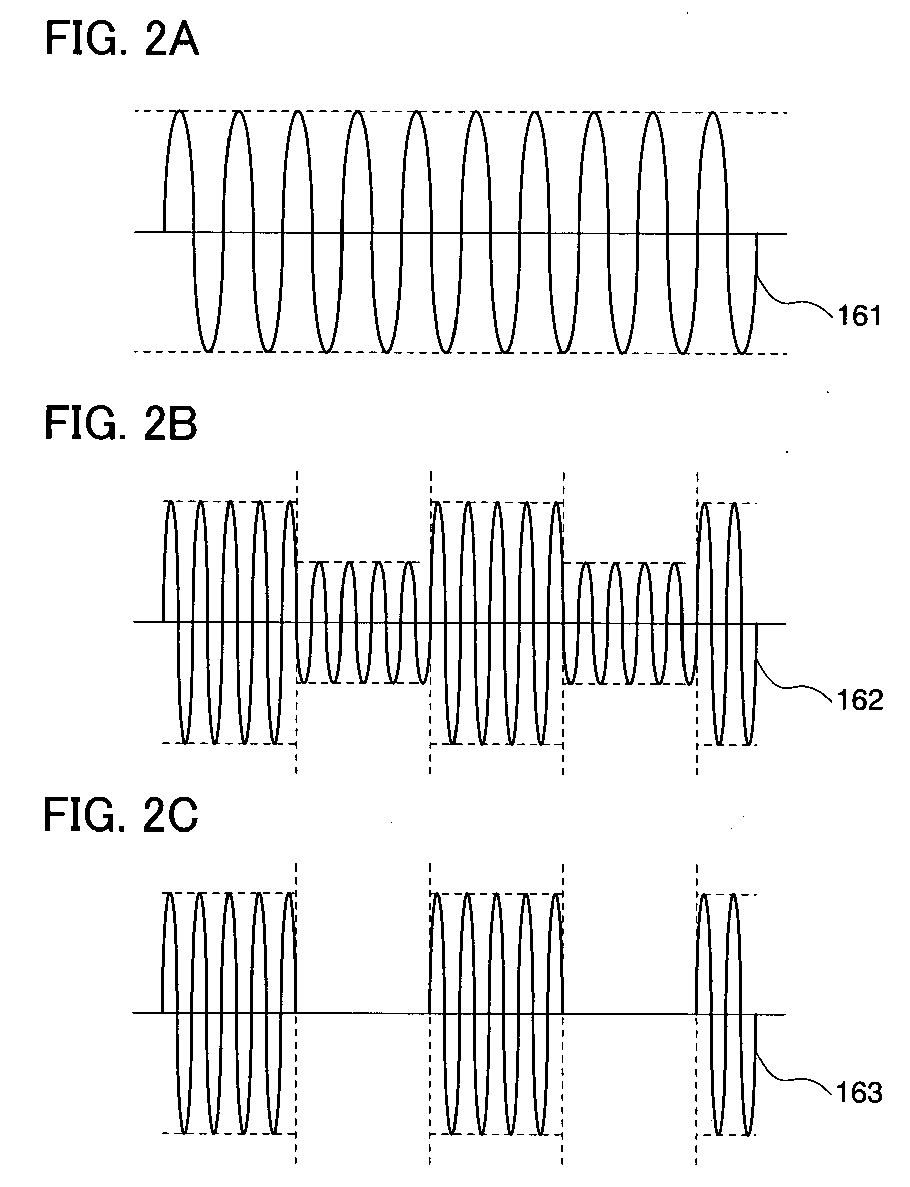
[0079]A transmission method for wireless communication signals depends on the frequency of the signals used for communication. For example, when the frequency is in the long wavelength region (for example, at a frequency band of 135 kHz or less) or in the shortwave band (for example, at the 13.56 MHz frequency band), the transmission method used is an electromagnetic coupling method or an electromagnetic induction method. On the other hand, when the frequency of the signals is in the UHF band (from 860 MHz to 930 MHz) or at the 2.45 GHz band, the transmission method used is a microwave method (also referred to as a radio wave method).

[0080]The shape of an antenna portion in an antenna circuit differs greatly depending on the transmission method used. For the electromagnetic coupling method or the electromagnetic induction method, because electromagnetic induction by variations in the magnetic field density is used, a conductor that functions as the antenna portion is a ring shape (f...

embodiment mode 3

[0098]In the present embodiment mode, as one feature of a semiconductor device of the present invention, an inlay that is used in an IC tag will be described. The inlay is an intermediate product for a final product of an IC tag or an IC card. The inlay is embedded in a plastic card, attached to a sticker label, or made into paper and used as an IC card, an ID label, or an IC tag.

[0099]FIG. 7, FIG. 8, FIG. 9, and FIG. 10 are perspective-view diagrams each illustrating an example of a structure of an inlay of the present embodiment mode. In each of FIG. 7, FIG. 8, FIG. 9, and FIG. 10, an example in which the structure of the antenna circuit 101 in FIG. 3 is used as an antenna circuit, but the antenna circuit shown in FIG. 4 or an antenna circuit with a different structure can be used. Hereinafter, structures of the inlays shown in FIG. 7, FIG. 8, FIG. 9, and FIG. 10 will be described.

[0100]FIG. 7 is an exploded-view perspective diagram of an inlay 400. A substrate 401 is a supporting...


PUM


Abstract

The semiconductor device includes a signal processing circuit, an antenna circuit that is connected to the signal processing circuit, and a storage means that supplies electric power to the signal processing circuit. The signal processing circuit receives and transmits information through the antenna circuit, generates a direct current voltage from signals received by the antenna circuit, and stores the direct current voltage in the storage means. Furthermore, the antenna circuit has an antenna portion that receives signals by an electromagnetic induction method and an antenna portion that receives signals by a microwave method so that signals of frequencies from a wide band can be received. Because signals from a wide band can be received, the environment in which the storage means can be charged is widened.

Description

BACKGROUND OF THE INVENTION[0001]1. Field of the Invention[0002]The present invention relates to a semiconductor device by which communication of data is performed wirelessly.[0003]2. Description of the Related Art[0004]In recent years, individual identification technology using wireless communication has been gathering attention. In particular, individual identification technology using RFID (radio frequency identification) tags as semiconductor devices by which exchange of data is performed by wireless communication has been gathering attention. RFID tags (hereinafter, simply called RFID) are also referred to as IC (integrated circuit) tags, IC chips, RF tags, wireless tags, and electronic tags. Individual identification technology using RFID has begun to be used in the production and management of individual objects, the identification of individual people, and the like.[0005]RFID can be divided into two types, active RFID in which electromagnetic waves that include RFID informat...

Claims


Application Information

Patent Timeline
IPC IPC(8): H04B7/00
CPCH01Q1/2225H01Q21/28H04B5/0081H04B5/0062H04B5/00
Inventor OSADA, TAKESHITAMURA, HIKARU
Owner SEMICON ENERGY LAB CO LTD
Why Eureka
Try Eureka