Circuit and method for cancellation of column pattern noise in CMOS imagers

a cmos imager and circuit technology, applied in the field of imaging devices, can solve the problems of ccd image sensors that are not easily integrated with cmos process peripheral circuitry, ccd image sensors also require relatively high power supply voltage, and require relatively high power to operate, so as to correct the non-linearity of isolated data

Active Publication Date: 2005-06-07
SMAL CAMERA TECH
View PDF41 Cites 101 Cited by
  • Summary
  • Abstract
  • Description
  • Claims
  • Application Information

AI Technical Summary

Benefits of technology

[0025]A first aspect of the present invention is a method for compensating non-linearity errors in A / D converter conversion operations associated with converting analog image data from a CMOS imager to digital data. The method isolates an A / D converter from the CMOS imager; applies a plurality of analog voltages to the isolated A / D converter, the plurality of voltages ranging from analog ground to a full-scale voltage level; measures and stories a difference between an output from the isolated A / D converter and a reference value associated with the analog voltage being applied to the isolated A / D converter; and corrects the non-linearity of the isolated the isolated A / D converter using the stored difference.

Problems solved by technology

For example, CCD image sensors are not easily integrated with CMOS process peripheral circuitry due to complex fabrication requirements and relatively high cost.
CCD images sensors also require relatively high power supply voltages and thus also require relatively high power to operate.
Despite these advantages, however, CMOS image sensors also have various disadvantages in comparison to CCD image sensors.
For example, the quality of image obtained by a CMOS imager is in general poorer compared with that from a CCD imager.
One of the contributing factors of poorer image quality in CMOS imagers is image pattern noise.
CMOS pattern noise is generally due to mismatches in the threshold voltages of the MOS transistors of a CMOS pixel, feedthrough of electronic charge, associated with the MOS pixel transistors, and mismatches in the processing circuits, including correlated double sampling amplifiers and analog-to-digital (A / D) converters.
However, both threshold mismatch and feedthrough noise compensation techniques do not remove image pattern noise that is due to mismatches in the processing circuits themselves.
The image pattern noise due to mismatches in the processing circuits typically has a columnar structure, and is more highly objectionable to human visualization than the random pixel-to-pixel fixed pattern noise due to threshold mismatches and feedthrough.
The output of the row of correlated double sampling circuits is then scanned rapidly by a horizontal shift register to read the line out to a common output port, thus any mismatch between the correlated double sampling circuits results in a column fixed pattern noise artifact in the captured image.
Such mismatches are typically caused by different DC offsets and gains in the signal amplification and processing provided by the correlated double sampling circuits.
As explained previously, mismatches in electrical characteristics among correlated double sampling amplifiers and A / D converters cause column pattern noise in the resulting image.
The resulting column pattern noise is because the electrical characteristics of the individual correlated double sampling amplifiers and A / D converters may be slightly different, due, e.g., to component mismatches.
Gain mismatch among correlated double sampling amplifiers or A / D converters also produces column pattern noise.
Since the error due to gain mismatch is a linear function of the input light intensity, the resulting column pattern noise is not fixed, but varies with input light intensity.
Errors in A / D converter conversion linearity can also give rise to similar column pattern noise.
In this case, the column pattern noise is also gained up by the same factor, making it more noticeable.
Since the error due to gain mismatches among correlated double sampling amplifiers or A / D converters and the linearity errors in A / D converters are small when the intensity is low, the column pattern noise is here generally dominated by offset errors in correlated double sampling amplifiers and A / D converters.
Although this technique does enable correction of the dark offset caused by both charge feedthrough and processing circuit mismatches, it requires the application of a calibration factor to the post-processing of images, thereby requiring extensive hardware.
This further modification adds substantial cost to the camera system.
As a result, for many applications, even this pattern noise compensation technique cannot be employed, and in general, compensation for non-fixed, gain-dependent cannot be achieved.

Method used


Image

  • Circuit and method for cancellation of column pattern noise in CMOS imagers
  • Circuit and method for cancellation of column pattern noise in CMOS imagers
  • Circuit and method for cancellation of column pattern noise in CMOS imagers

Examples


Embodiment Construction

[0031]The present invention will be described in connection with preferred embodiments; however, it will be understood that there is no intent to limit the present invention to the embodiments described herein. On the contrary, the intent is to cover all alternatives, modifications, and equivalents as may be included within the spirit and scope of the present invention as defined by the appended claims.

[0032]For a general understanding of the present invention, reference is made to the drawings. In the drawings, like reference numbering has been used throughout to designate identical or equivalent elements. It is also noted that the various drawings illustrating the present invention are not drawn to scale and that certain regions have been purposely drawn disproportionately so that the features and concepts of the present invention could be properly illustrated.

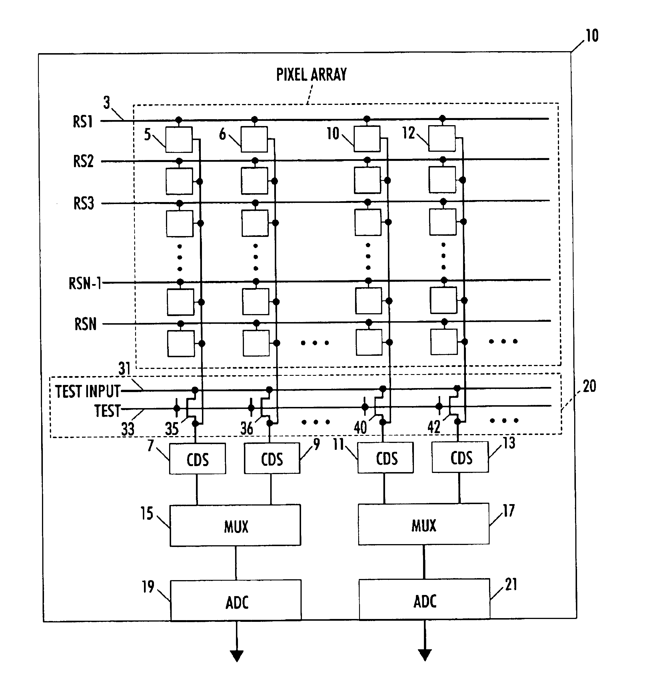
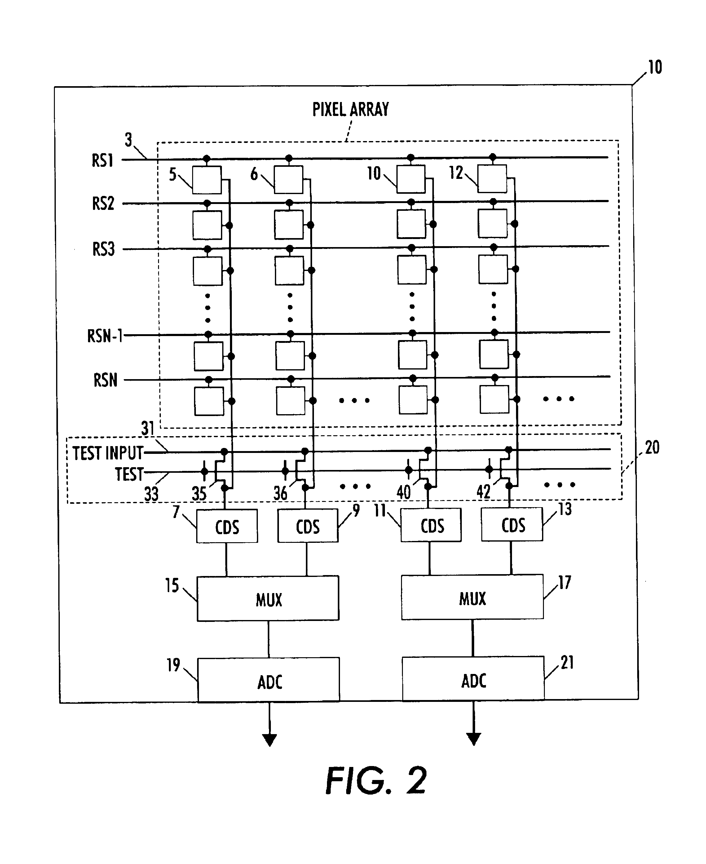
[0033]In accordance with the concepts of the present invention, FIG. 2 schematically illustrates a CMOS imager 10 of the i...


PUM


Abstract

A circuit and method measure the output voltage of a CMOS pixel in a manner that substantially reduces all columnar pattern noise due to mismatches in the signal processing circuits including the correlated double sampling amplifiers and A/D converters. The circuit includes a test switch, operatively connected between a reference voltage source and a correlated double sampling amplifier, for applying a test voltage from the reference voltage source when the state of the test switch is ON to the correlated double sampling amplifier. The reference voltage source produces a voltage corresponding to a full-scale voltage level to enable the determination of a gain error in the correlated double sampling amplifier and/or A/D converter; a voltage corresponding to ground to enable the determination of an offset error in the correlated double sampling amplifier and/or A/D converter; and a plurality of analog voltages ranging from analog ground to a full-scale voltage level to enable the determination of non-linearity errors in the A/D converter.

Description

PRIORITY INFORMATION[0001]This application claims priority from U.S. Provisional Patent Application, Ser. No. 60 / 416,043, filed on Oct. 4, 2002. The entire contents of U.S. Provisional Patent Application, Ser. No. 60 / 416,043 are hereby incorporated by reference.FIELD OF THE PRESENT INVENTION[0002]The present invention relates to imaging devices and, in particular, to complementary metal-oxide semiconductor (CMOS) image sensors with reduced fixed pattern noise.BACKGROUND OF THE PRESENT INVENTION[0003]Various types of imagers or image sensors are in use today, including charge-coupled device (CCD) image sensors and complementary metal-oxide semiconductor CMOS image sensors. CMOS image sensors typically utilize an array of active pixel image sensors and a row or register of correlated double-sampling circuits or amplifiers to sample and hold the output of a given row of pixel image sensors of the array. Each active pixel image sensor of the array of pixels typically contains a pixel-am...

Claims


Application Information

Patent Timeline
Patent Type & Authority Patents(United States)
IPC IPC(8): H03M1/10H03M1/12
CPCH03M1/1038H03M1/123
Inventor LEE, HAE-SEUNGFIFE, KEITH GLEN
Owner SMAL CAMERA TECH
Why Eureka
Try Eureka