Measuring Apparatus

a technology of measuring apparatus and measuring rod, which is applied in the direction of weighing apparatus, instruments, electric digital data processing, etc., can solve problems such as fabrication errors

Inactive Publication Date: 2011-05-19
METRYX
View PDF19 Cites 2 Cited by
  • Summary
  • Abstract
  • Description
  • Claims
  • Application Information

AI Technical Summary

Benefits of technology

[0017]Preferably, the wafer is substantially horizontal during measurement to minimise errors. The pivot element and weighing unit may therefore include support surface or elements adapted to contact the underside of the wafer.
[0026]The probe may be movable between detection points on the back of the wafer by dragging across the lower surface of the wafer. Preferably a low friction mechanism, e.g. a PTFE wheel as the probe tip, is provided between the probe and the lower surface of the wafer to prevent or minimize any effect on the mass distribution of the wafer that the tracking will have. The force exerted on the weighing unit due the moment of the wafer may be measured in a continuous fashion as the probe is moved across the back surface of the wafer.
[0027]Alternatively, the probe may be applied discretely at each of the detection points. In this case, there is no direct rubbing between the probe and back surface of the wafer, which can avoid problems associated with depositing or removing particles from the wafer.

Problems solved by technology

However, such devices are arranged only to detect the total mass of the wafers.
However, in practice, the value measured by the weighing detector gives a good indication of the likelihood of errors in fabrication.

Method used


Image

  • Measuring Apparatus
  • Measuring Apparatus
  • Measuring Apparatus

Examples


Embodiment Construction

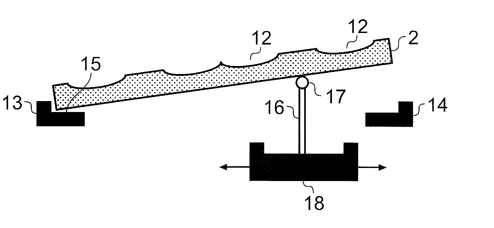
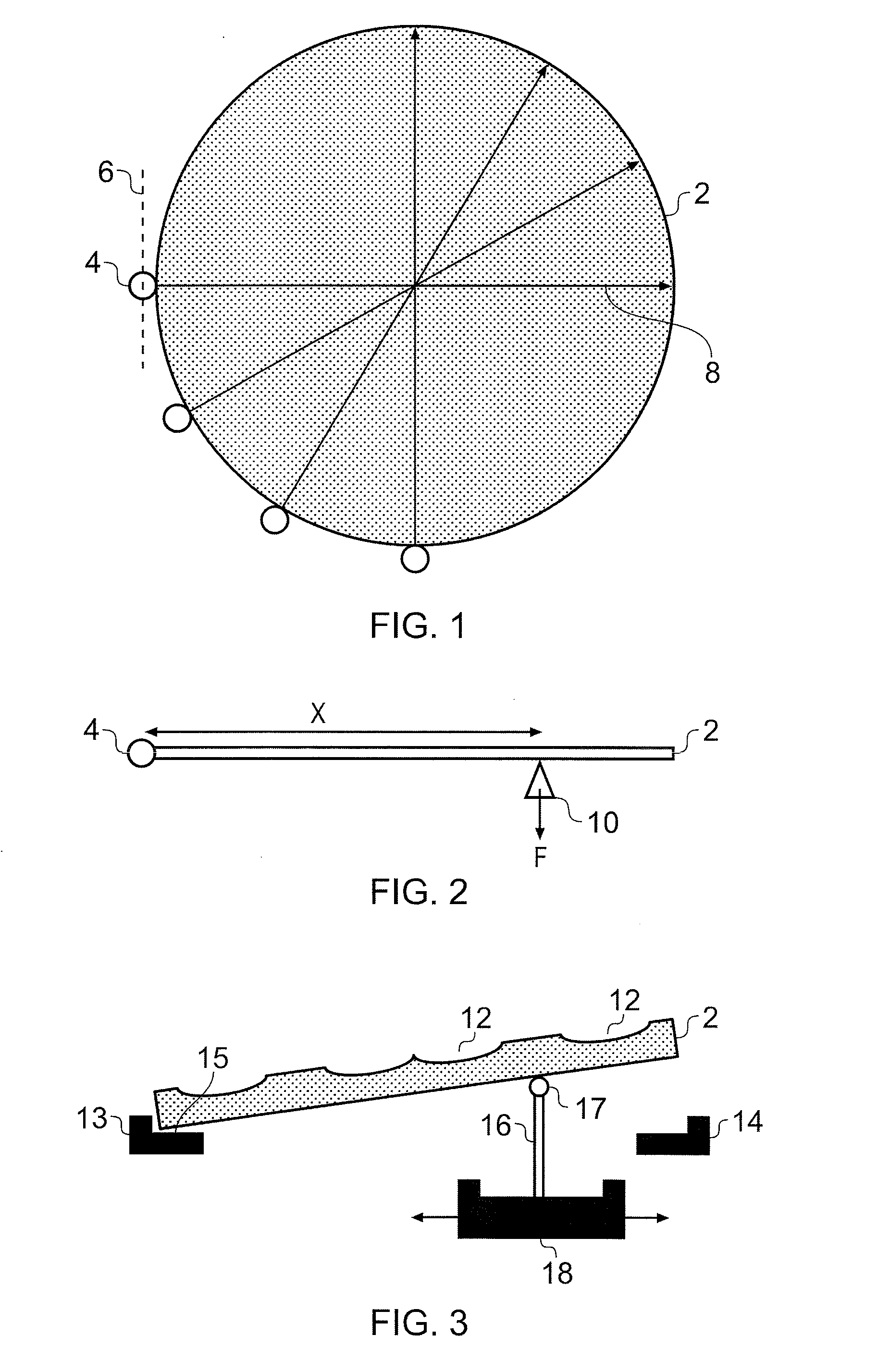
[0038]FIG. 1 shows a plan view of a wafer measurement process according to the present invention. A circular semiconductor wafer 2 is pivotally supported on its edge. The wafer 2 can pivot about a plurality of fulcrums 4 around the edge (circumference) of the wafer 2. FIG. 1 illustrates four positions for the fulcrum 4. For a perfectly uniform wafer, the centre of mass is at the centre of the wafer and the wafer is pivotable about a pivot axis 6 at each fulcrum that is normal to a diameter 8.

[0039]FIG. 2 shows a side view of the arrangement shown in FIG. 1. The wafer 2 is freely pivotable about the fulcrum 4, but is supported in a horizontal orientation by weighing probe 10. The probe 10 is attached to a force sensor (not shown) to detect the force exerted by the weight of the wafer 2 and thereby calculate the moment of the wafer 2 about the fulcrum 4. In FIG. 2, the moment is the sensed force F multiplied by the distance x to the fulcrum 4.

[0040]The probe 10 is movable to take mome...


PUM


Abstract

Measuring apparatus for monitoring the position of the centre of mass of a semiconductor wafer is disclosed. The apparatus includes a wafer support (14) with a ledge for supporting an edge of a wafer (2) when it is lifted at a detection point by a probe (16). The probe (16) is connected to a force sensor (18) which senses a force due to a moment of the wafer about a fulcrum (4) on the wafer support (14). Moment measurements are taken at a plurality of detection points and a processing unit calculates the position of the centre of mass from the moment measurements. Changes in wafer mass distribution (e.g. due to faulty treatment steps) which cause movement of the centre of mass can be detected.

Description

CROSS REFERENCE TO RELATED APPLICATIONS[0001]This application is a divisional application of U.S. application Ser. No. 11 / 868,746, filed Oct. 8, 2007 (which is hereby incorporated by reference).FIELD OF THE INVENTION[0002]The present invention relates to measuring apparatus for monitoring the fabrication process of a semiconductor wafer.BACKGROUND OF THE INVENTION[0003]Microelectronic devices are fabricated on semiconductor wafers using a variety of techniques, e.g. including deposition techniques (CVD, PECVD, PVD, etc) and removal techniques (e.g. chemical etching, CMP, etc). Semiconductor e.g. silicon wafers may be further treated in ways that alter their mass distribution e.g. by cleaning, ion implantation, lithography and the like. These treatment techniques typically cause a change in the mass distribution at or on the surface of the semiconductor wafer. The configuration of the changes to the surface are often vital to the functioning of the device, so it is desirable for qual...

Claims


Application Information

Patent Timeline
Patent Type & Authority Applications(United States)
IPC IPC(8): G06F19/00G01G19/00
CPCG01G19/00G01G17/00G01G21/28
Inventor WILBY, ROBERT JOHNKIERMASZ, ADRIAN
Owner METRYX
Why Eureka
Try Eureka