Light-emitting element and organic electroluminescent display device

a technology of light-emitting elements and display devices, which is applied in the direction of organic semiconductor devices, electroluminescent light sources, electric lighting sources, etc., can solve the problems that the above-mentioned problems cannot be solved

Inactive Publication Date: 2011-05-26
SONY CORP
View PDF5 Cites 32 Cited by
  • Summary
  • Abstract
  • Description
  • Claims
  • Application Information

AI Technical Summary

Benefits of technology

[0056]What is more, in the light-emitting elements in the first to sixth aspects of the invention, or in the organic EL display device of the invention, as to the characteristics of the light-emitting elements or those of the organic EL elements, the same level of reliability as that of the pr...

Problems solved by technology

The concern here is that, as described in these published unexamined patent applications, even if a high-resistance layer is provided by ins...

Method used


Image

  • Light-emitting element and organic electroluminescent display device
  • Light-emitting element and organic electroluminescent display device
  • Light-emitting element and organic electroluminescent display device

Examples


first embodiment

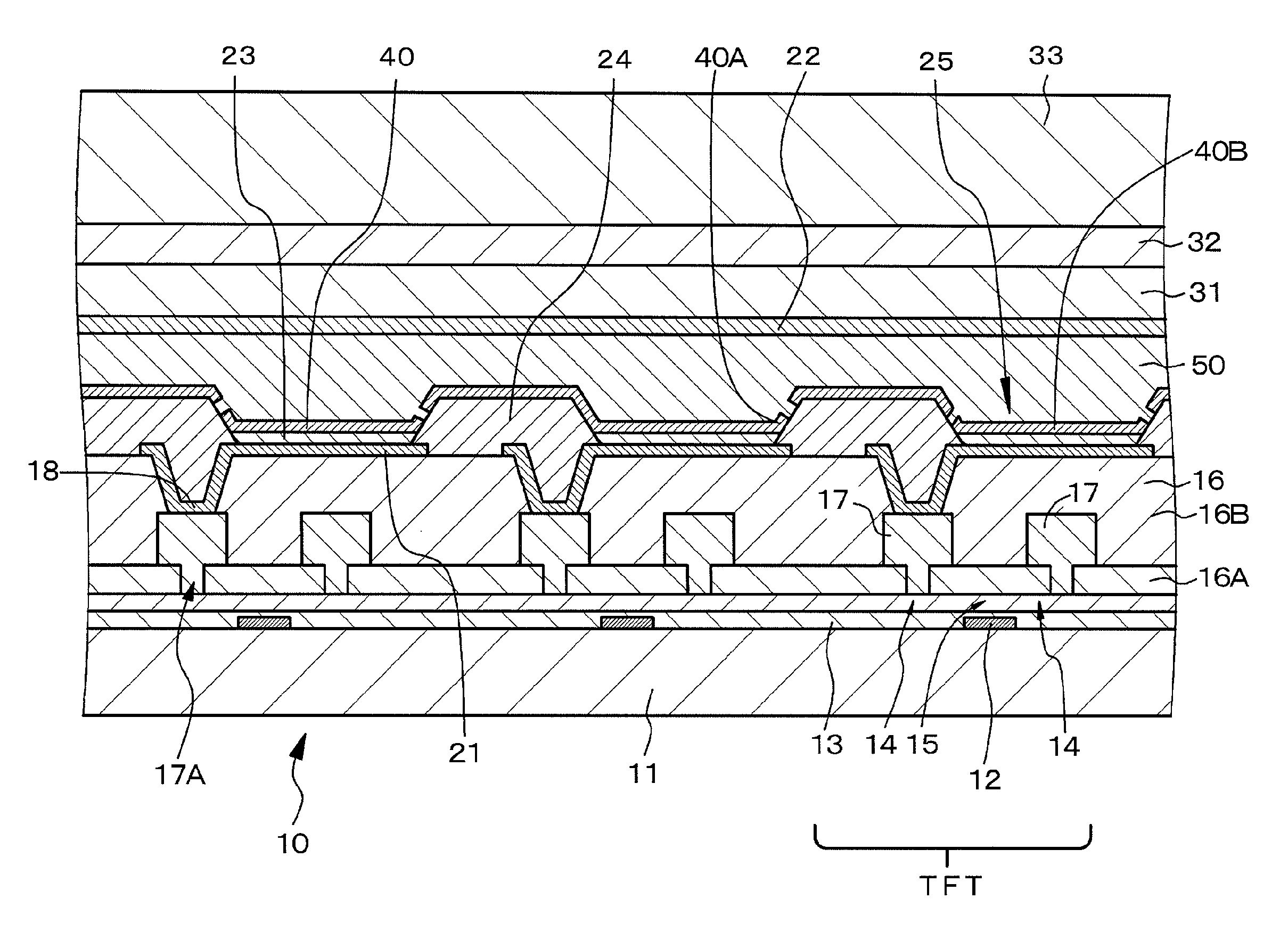
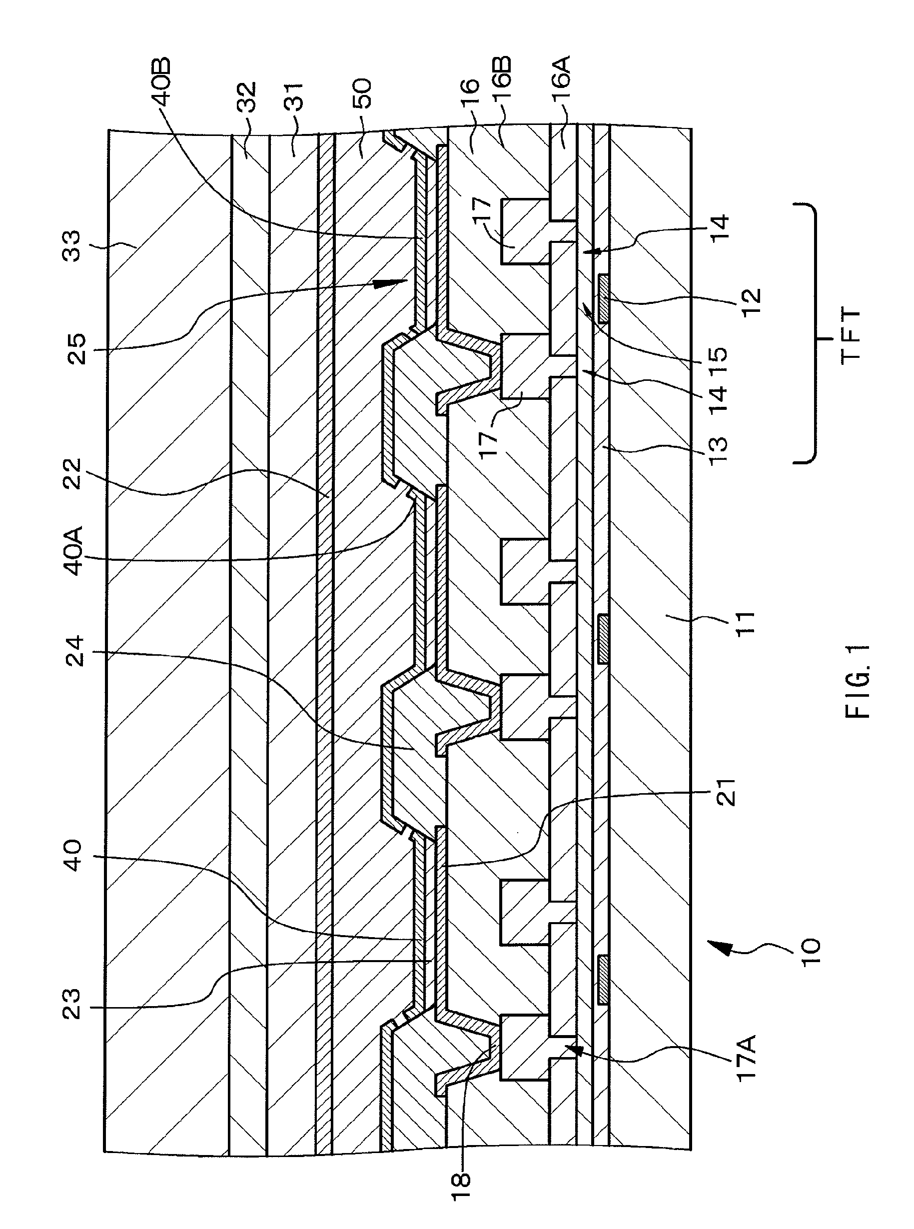
[0071]A first embodiment is related to light-emitting elements in first to sixth aspects of the invention, and to an organic EL display device of the invention. FIG. 1 shows a schematic partial cross sectional view of the organic EL display device of the first embodiment, and FIGS. 2(A) and (B) each show a schematic view of an organic layer or others. The organic EL display device of the first embodiment is an active-matrix organic EL display device for color display, and is of a top emission type. In other words, through a second electrode, and also through a second substrate, a light is emitted.

[0072]The organic EL display device of the first embodiment includes a plurality of (e.g., N×M=2880×540) light-emitting elements (to be specific, organic EL elements) 10. Note that one light-emitting element (organic EL element) 10 configures one sub pixel. Accordingly, the organic EL display device includes (N×M) / 3 pixels. Herein, one pixel is configured by three types of sub pixels, inclu...

second embodiment

[0138]A second embodiment is a modification of the first embodiment, and therein, a resistance layer is in the lamination configuration including first and second resistance layers from the side of an organic layer, and the second resistance layer has the electrical resistivity higher than that of the first resistance layer. In this second embodiment, the first and second resistance layers are both made of Nb2O5, and by changing the partial pressure of oxygen during the film formation by sputtering using Nb2O5, the first and second resistance layers respectively have the values of electrical resistivity R1 and R2 as below.

[0139]Electrical resistivity R1 of First resistance layer: 1×10⁶Ω·m (1×10⁴ Ω·cm)

[0140]Electrical resistivity R2 of Second resistance layer: 1×10⁸ Ω·m (1×10⁶ Ω·cm)

[0141]When the resistance layer is measured for a voltage drop therein, in comparison with the measurement result of voltage drop in a resistance layer configured by a single layer (electrical resistivity:...

third embodiment

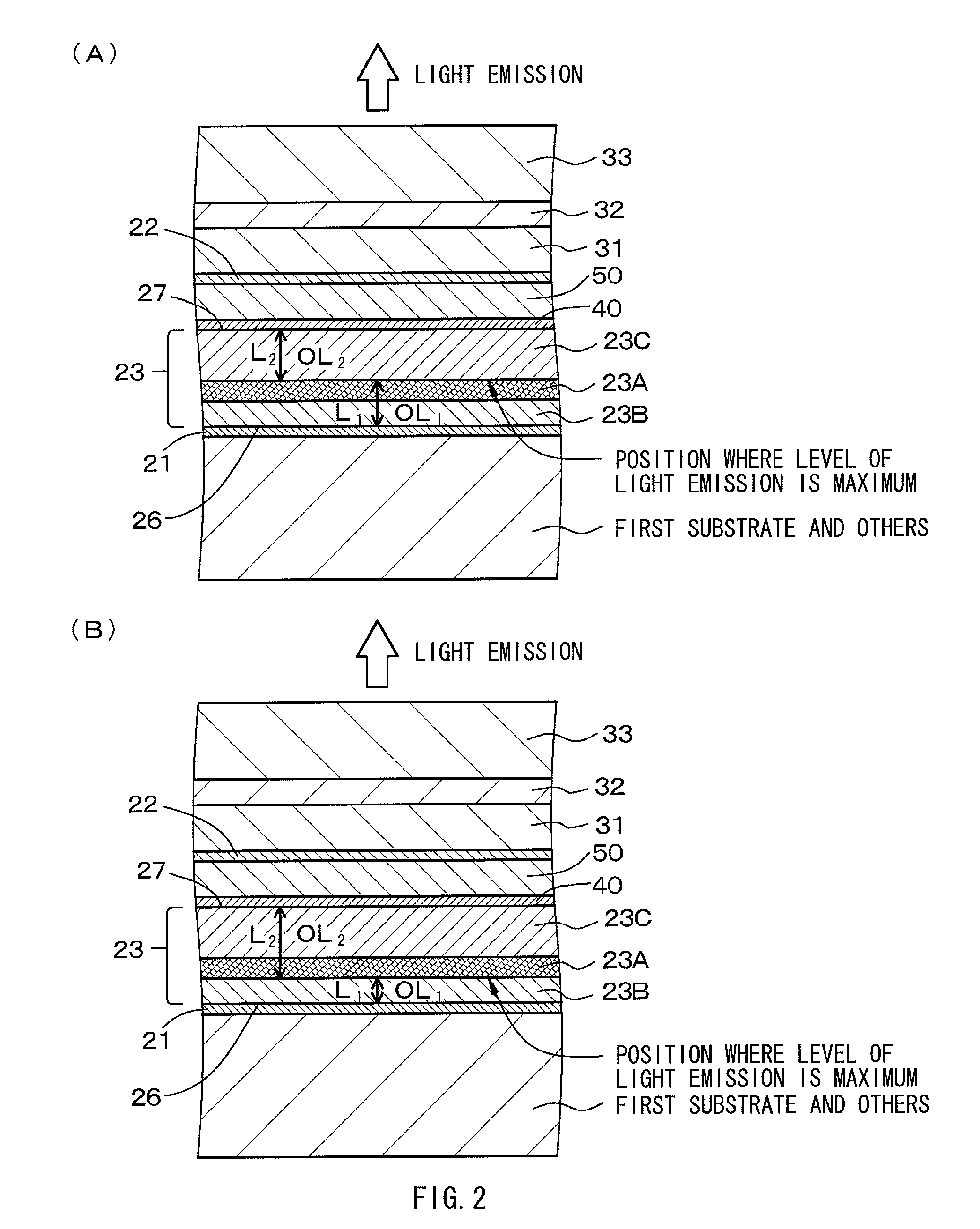
[0143]A third embodiment is also a modification of the first embodiment. In the first embodiment, the part of the resistance layer positioned above the red light-emitting sub pixel may have the electrical resistance value (electrical resistance value per unit area of the resistance layer. The same is applicable to below) RR, which is the same as the electrical resistance value RG of the part of the resistance layer positioned above the green light-emitting sub pixel, and as the electrical resistance value RB of the part of the resistance layer positioned above the blue light-emitting sub pixel. In other words, the entire surface is covered uniformly by the resistance layer. Herein, generally, the blue light-emitting sub pixel with a short wavelength of light emission has the optical distance LB shorter than optical distances LG and LR respectively for the green light-emitting sub pixel and the red light-emitting sub pixel each with a longer wavelength of light emission. Therefore, t...


PUM


Abstract

Provided is a light-emitting element in the structure and configuration of causing no possibility of a short circuit between first and second electrodes even if there is any foreign substance or a protrusion on the first electrode. Such a light-emitting element is configured to include, in order, a first electrode 21, an organic layer 23 including a light-emitting layer made of an organic light-emitting material, a semi-transmissive/reflective film 40, a resistance layer 50, and a second electrode 22. The first electrode 21 reflects a light coming from the light-emitting layer, and the second electrode 22 passes through a light coming from the semi-transmissive/reflective film 40 after passing therethrough. The semi-transmissive/reflective film on the organic layer 23 has an average film thickness of 1 nm to 6 nm both inclusive.

Description

TECHNICAL FIELD[0001]The present invention relates to a light-emitting element in the configuration of a resonator, and an organic electroluminescent display device provided therein with this light-emitting element.BACKGROUND ART[0002]In recent years, as a display device for alternative use of a liquid crystal display device, an organic electroluminescent display device (organic EL display device) using organic electroluminescent elements (organic EL elements) are receiving attention. The organic EL display device is of a self-luminous type, and has characteristics of low power consumption. It is also considered as having the response characteristic of a sufficient level also with respect to a high-speed video signal with high definition, and thus is under active development for practical use thereof.[0003]The organic EL element generally has the lamination configuration in which a first electrode, an organic layer, and a second electrode are disposed one on the other. The organic l...

Claims


Application Information

Patent Timeline
IPC IPC(8): H01L51/52
CPCH01L27/3244H01L27/3276H01L51/5234H01L51/5203H01L2251/5315H01L2251/558H05B33/24H01L51/5265H10K59/12H10K59/131H10K50/828H10K50/852H10K2102/3026H10K2102/351H05B33/28H10K50/805
Inventor YAMADA, JIRONEGISHI, EISUKENAKAMURA, HIROFUMINAKAMURA, AKIFUMIYOSHINAGA, TADAHIKO
Owner SONY CORP
Why Eureka
Try Eureka