High-Speed Ceramic Modules with Hybrid Referencing Scheme for Improved Performance and Reduced Cost

a ceramic module and hybrid referencing technology, applied in the field of integrated circuit packaging, can solve the problems of limited metal area versus total area of the layer, yield problems, etc., and achieve the effect of widening the mesh pitch and high power usag

Active Publication Date: 2011-06-09
TAIWAN SEMICON MFG CO LTD
View PDF19 Cites 10 Cited by
  • Summary
  • Abstract
  • Description
  • Claims
  • Application Information

AI Technical Summary

Benefits of technology

The patent describes a multi-layered ceramic package that has high power usage areas and non-high power usage areas. The package includes a signal layer, a voltage power layer, and a ground layer. The voltage power layer and ground layer are directly adjacent to the signal layer and provide reference mesh planes. The package also includes a hybrid mesh scheme, which consists of three mesh densities: a full dense mesh in the areas adjacent to the high power usage areas, a half dense mesh in the areas adjacent to the perimeter edges of the high power usage areas, and a low density mesh in all other areas. The low density mesh provides a wider mesh pitch. The voltage power and ground layers have aligned traces that run parallel to adjacent signal lines in the non-high power usage areas. The technical effect of this patent is to improve the performance and reliability of ceramic packages by optimizing the placement of power and ground layers and reducing interference between signal lines.

Problems solved by technology

The technical problem addressed in this patent text is the limited metal loading in ceramic packages designed with mesh planes, which can result in higher crosstalk coefficients and yield issues. This limitation affects the manufacturing cost of the ceramic modules and requires a certain amount of copper paste for manufacturing.

Method used


Image

  • High-Speed Ceramic Modules with Hybrid Referencing Scheme for Improved Performance and Reduced Cost
  • High-Speed Ceramic Modules with Hybrid Referencing Scheme for Improved Performance and Reduced Cost
  • High-Speed Ceramic Modules with Hybrid Referencing Scheme for Improved Performance and Reduced Cost

Examples


Embodiment Construction

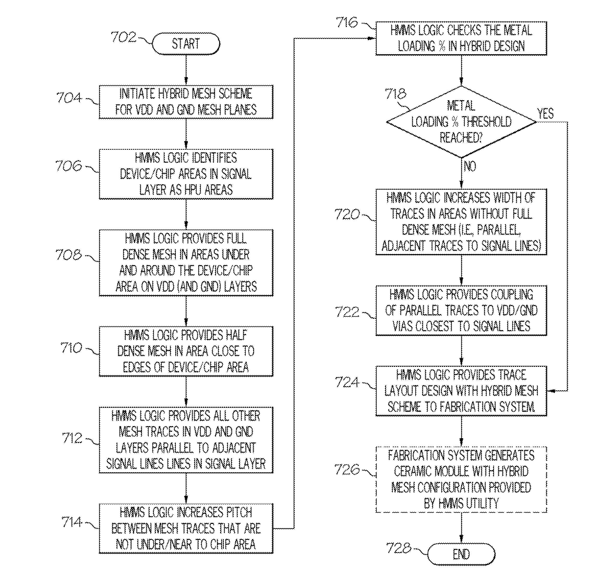
[0016]As described herein, the embodiments provide a multi-layered ceramic package, as well as, a method, a fabrication system / device and a computer program product for providing a hybrid mesh scheme within the reference Vdd and Gnd mesh layers to enable good power delivery to chips / devices within the signal layer sandwiched between the Vdd and Gnd layers. Fabrication of the ceramic package via implementation of the method and / or execution of the program product within a fabrication system further yields low metal loading and consequently lower cost for manufacturing the resulting ceramic packages / modules. Finally, the resulting ceramic packages / modules exhibit low far end (FE) noise / crosstalk relative to standard designs.

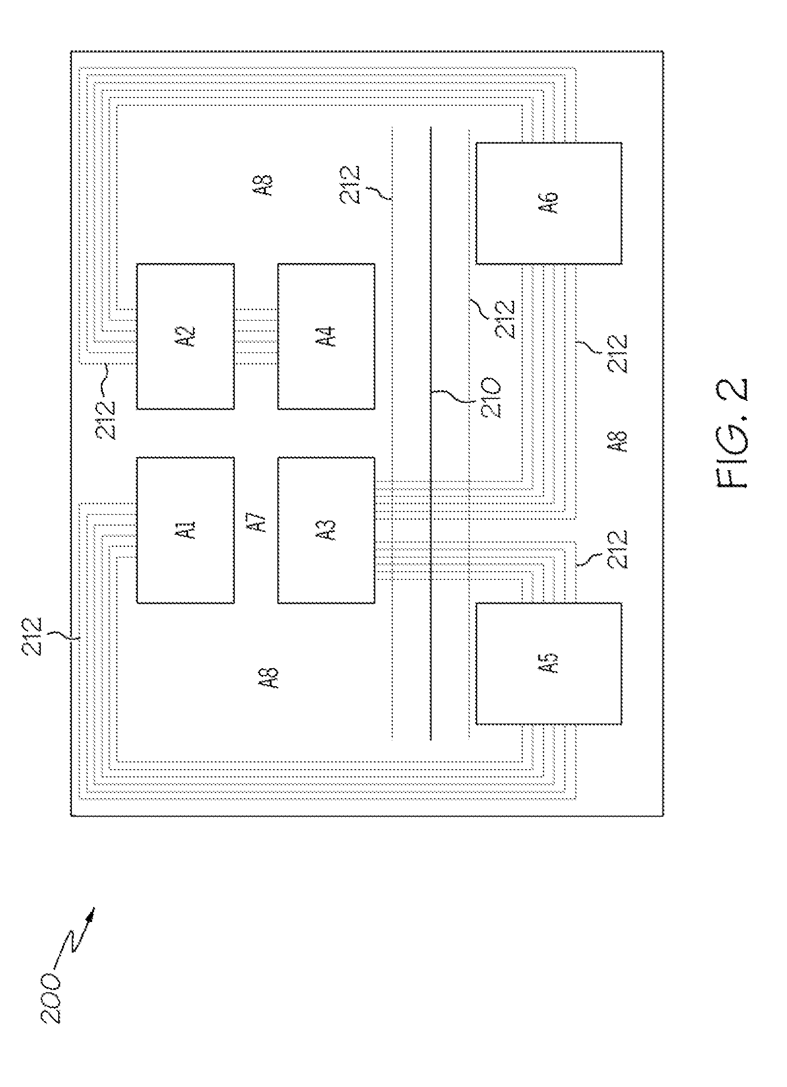
[0017]The illustrative embodiments provide an improved multi-layered ceramic package, which comprises: a signal layer with high power usage (HPU) areas (i.e., identified chip / device areas that require a supply of power) and one or more non-HPU areas; a voltage powe...


PUM

PropertyMeasurementUnit
Thicknessaaaaaaaaaa
Densityaaaaaaaaaa
Widthaaaaaaaaaa

Abstract

A multi-layered ceramic package comprises: a signal layer with identified chip/device area(s)/site(s) that require a supply of power; and a voltage power (Vdd) layer and a ground (Gnd) layer disposed on opposite sides directly above or below (adjacent to) the signal layer and providing a first reference mesh plane and a second reference mesh plane configured utilizing a hybrid mesh scheme. The hybrid mesh scheme comprises different mesh configurations from among: a full dense mesh in a first area directly above or below the identified chip/device area(s); a half dense mesh in a second area that is above or below the edge(s) of the chip/device area; and a wider mesh pitch in all other areas, and the Vdd traces are aligned to run parallel and adjacent to signal lines in those other areas. Wider traces are provided within the mesh areas that run parallel and adjacent to signal lines.

Description


Claims


Application Information

Patent Timeline
Owner TAIWAN SEMICON MFG CO LTD
Why Eureka
Try Eureka