Display panel device, display device, and control method thereof

a display panel and display device technology, applied in the field of display panel devices, display devices, and control methods thereof, can solve problems such as poor shading and variation among pixel units, and achieve the effect of suppressing variation in mobility correction and lowering the influence of wiring delay

Active Publication Date: 2011-06-16
JOLED INC
View PDF7 Cites 12 Cited by
  • Summary
  • Abstract
  • Description
  • Claims
  • Application Information

AI Technical Summary

Benefits of technology

[0030]With the display panel device, the display device, and the control method thereof in the present invention, the influence due to the wiring delay can be lowered by reducing the variation cau

Problems solved by technology

As described, due to the wiring delay of the scanning line WS, the mobility correction period T does not actually become the design value T0 of the correction period, which results in causing the variations among the pixel units.
Hence, there is a problem that when a wiring delay of t

Method used


Image

  • Display panel device, display device, and control method thereof
  • Display panel device, display device, and control method thereof
  • Display panel device, display device, and control method thereof

Examples


embodiment 1

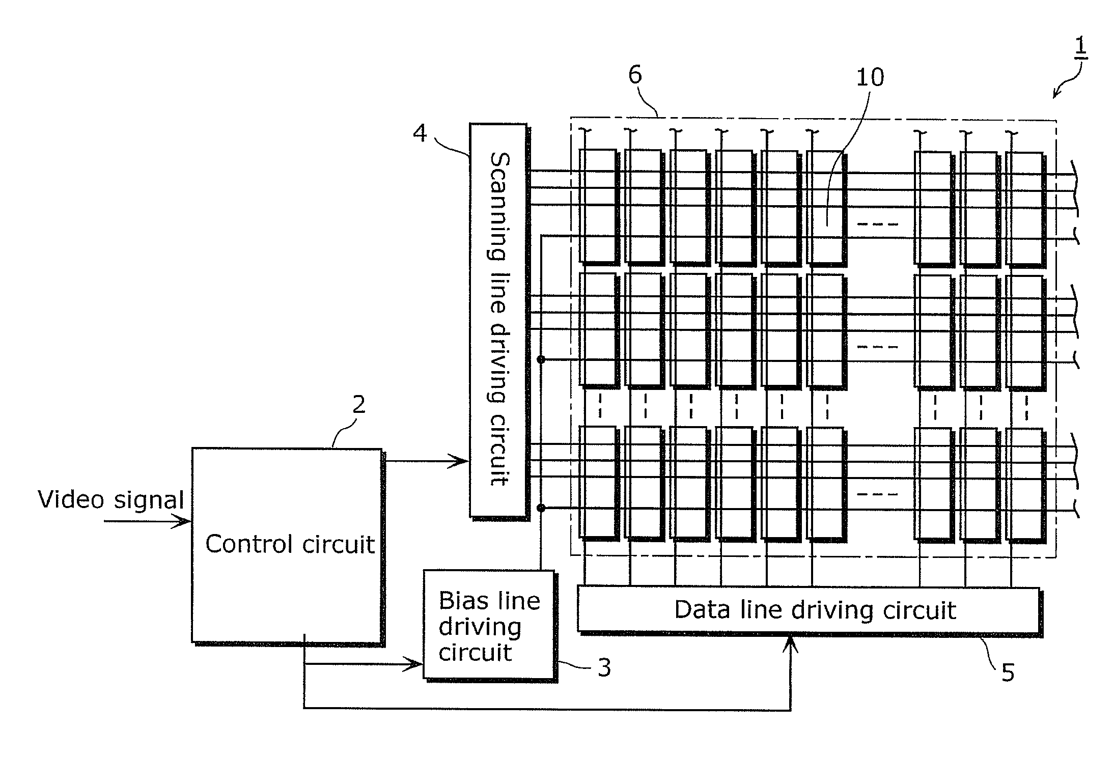
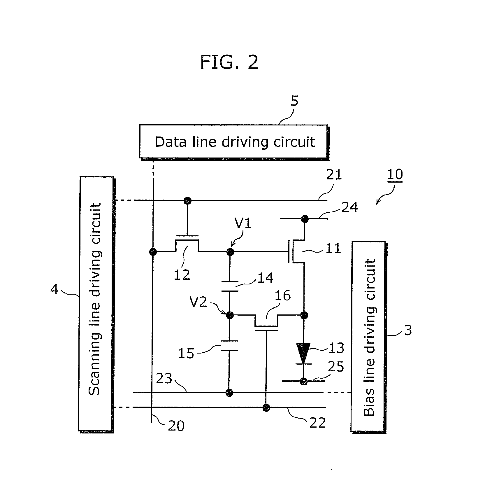
[0081]A display panel device according to an implementation of the present embodiment includes: organic EL elements; capacitors; driving transistors which cause drain current corresponding to voltage held by the capacitors to flow through the organic EL elements; data lines for supplying signal voltage; selecting transistors which switch between conduction and non-conduction between the data lines and the first capacitor electrodes of the capacitors; switching transistors which switch conduction and non-conduction between the source electrodes of the driving transistors and the second capacitor electrodes of first capacitors; and controllers.

[0082]The controller turns ON the switching transistor so that conduction is caused between the source electrode of the driving transistor and the second capacitor electrode of the capacitor. Then, the selecting transistor is turned ON so that signal voltage is supplied to the first capacitor electrode of the capacitor and that drain current of ...

embodiment 2

[0149]A display panel device in the present embodiment is different from the display panel device in Embodiment 1 in the pixel circuit configuration and in the driving timing thereof. In addition, the display panel device in the present embodiment does not include the bias line driving circuit 3. The pixel circuit configuration of the pixel circuit 30 in the present embodiment differs from that of the pixel circuit 10 in Embodiment 1 in that the capacitor 15 and the bias line 23 are not included, but instead, a switching transistor 17 and a scanning line 26 are added. Hereinafter, descriptions of similarities to the circuit configuration according to Embodiment 1 are omitted, and only differences from the circuit configuration in Embodiment 1 are described.

[0150]FIG. 10 is a diagram showing a circuit configuration of a luminescence pixel included in a display unit and connections with the surrounding circuits according to Embodiment 2 of the present invention. The luminescence pixel...


PUM


Abstract

A display panel device includes: a luminescence element; a capacitor including first and second capacitor electrodes; a driver having a gate connected to the first capacitor electrode for allowing a drain current to flow through the luminescence element; a first switch switchably interconnecting a data line and the first capacitor electrode for supplying a signal voltage to the capacitor; a second switch switchably interconnecting a source of the driver and the second capacitor electrode; and a controller. The controller is configured to: turn ON the first switch while the second switch is ON to supply the signal voltage to the first capacitor electrode and flow a current between the source of the driver and the second capacitor electrode; and, after predetermined time period, turn OFF the second switch to cause non-conduction between the source of the driver and the second capacitor electrode.

Description

CROSS REFERENCE TO RELATED APPLICATION[0001]This is a continuation application of PCT application No. PCT / JP2009 / 006213 filed Nov. 19, 2009, designating the United States of America, the disclosure of which, including the specification, drawings and claims, is incorporated herein by reference in its entirety.BACKGROUND OF THE INVENTION[0002]1. Field of the Invention[0003]The present invention relates to display panel devices, display devices, and control methods thereof, and in particular, to a display panel device and a display device using current-driven luminescence elements and a control method thereof.[0004]2. Description of the Related Art[0005]Image display devices using organic electro-luminescence (EL) elements are known as image display devices using current-driven luminescence elements. The organic EL display devices using self-luminous organic EL elements are best suited to make thinner devices because such organic EL elements do not require backlights conventionally req...

Claims


Application Information

Patent Timeline
IPC IPC(8): G06F3/038G09G3/30
CPCG09G3/3233G09G2300/0852G09G2320/0223G09G2310/0251G09G2300/0876H10K59/179H10K59/131
Inventor MATSUI, MASAFUMIONO, SHINYA
Owner JOLED INC
Why Eureka
Try Eureka