Display device having optical sensors

Inactive Publication Date: 2011-06-16
SHARP KK
View PDF25 Cites 28 Cited by
  • Summary
  • Abstract
  • Description
  • Claims
  • Application Information

AI Technical Summary

Benefits of technology

[0019]According to the first or eleventh aspect of the present invention, when a reflection image of an object is detected, the amount of light (reflected light) detected by the optical sensors is made larger during the sensing period than during the display period, whereby, while the power consumption of the backlight is suppressed, the luminance of the reflection image increases, enabling to increase the detection accuracy for a touch position.
[0020]According to the second aspect of the present invention, by selecting a suitable operating mode according to the conditions and making the amount of light (reflected light) detected by the optical sensors larger during the sensing period than during the display period in the reflection image mode, while the power consumption of the backlight is suppressed, the luminance of a reflection image increases, enabling to increase the detection accuracy for a touch position in the reflection image mode.
[0021]According to the third aspect of the present invention, by setting the luminance of the backlight higher during the sensing period than during the display period in the reflection image mode, the amount of light (reflected light) detected by the optical sensors can be increased. With this, while the power consumption of the backlight is suppressed, the luminance of a reflection image increases, enabling to increase the detection accuracy for a t

Problems solved by technology

However, in the method of detecting a shadow image, when the illumination of outside light is low (the surroundings are dark), it may become difficult to disting

Method used


Image

  • Display device having optical sensors
  • Display device having optical sensors
  • Display device having optical sensors

Examples


Example

First Embodiment

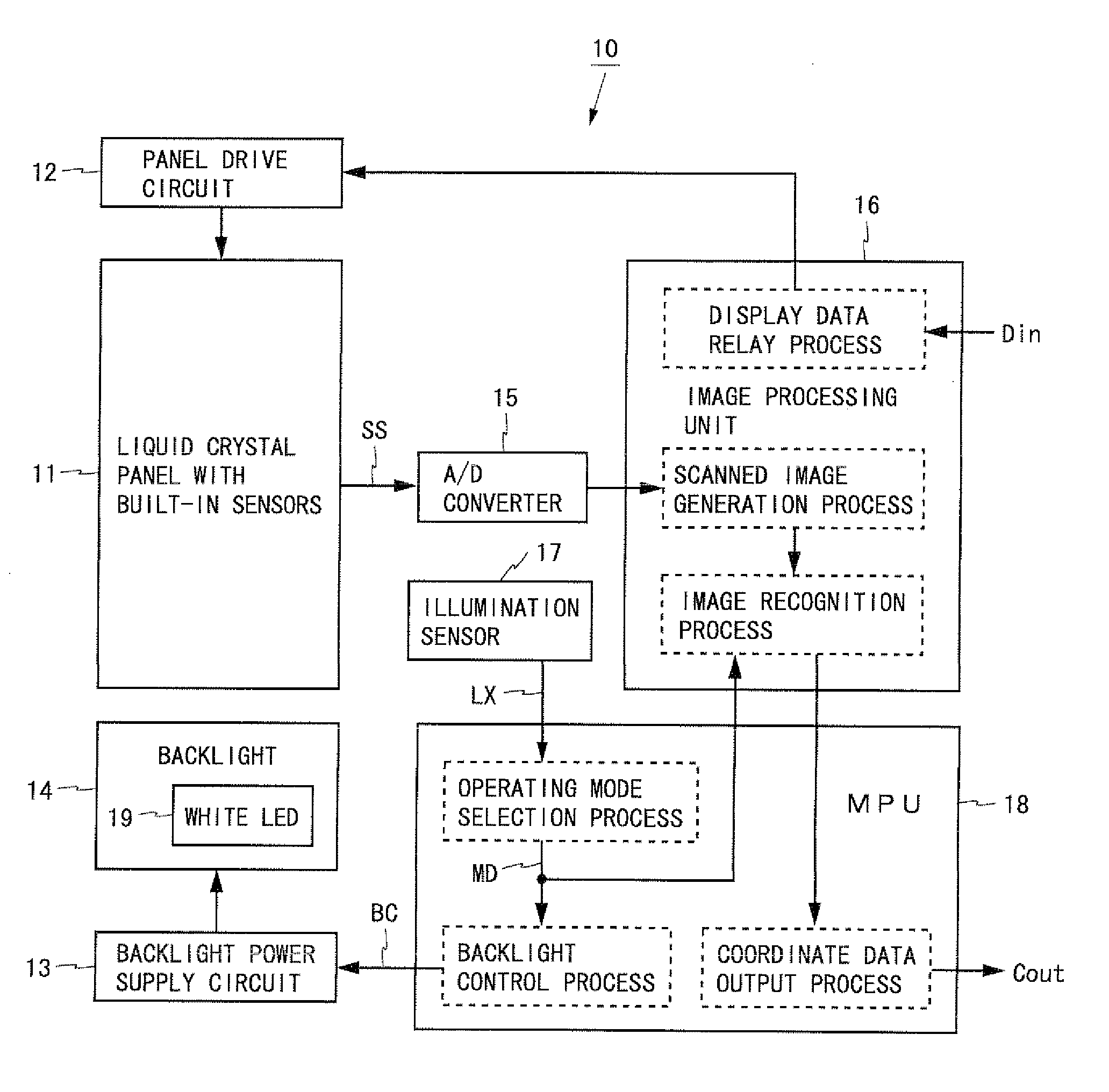
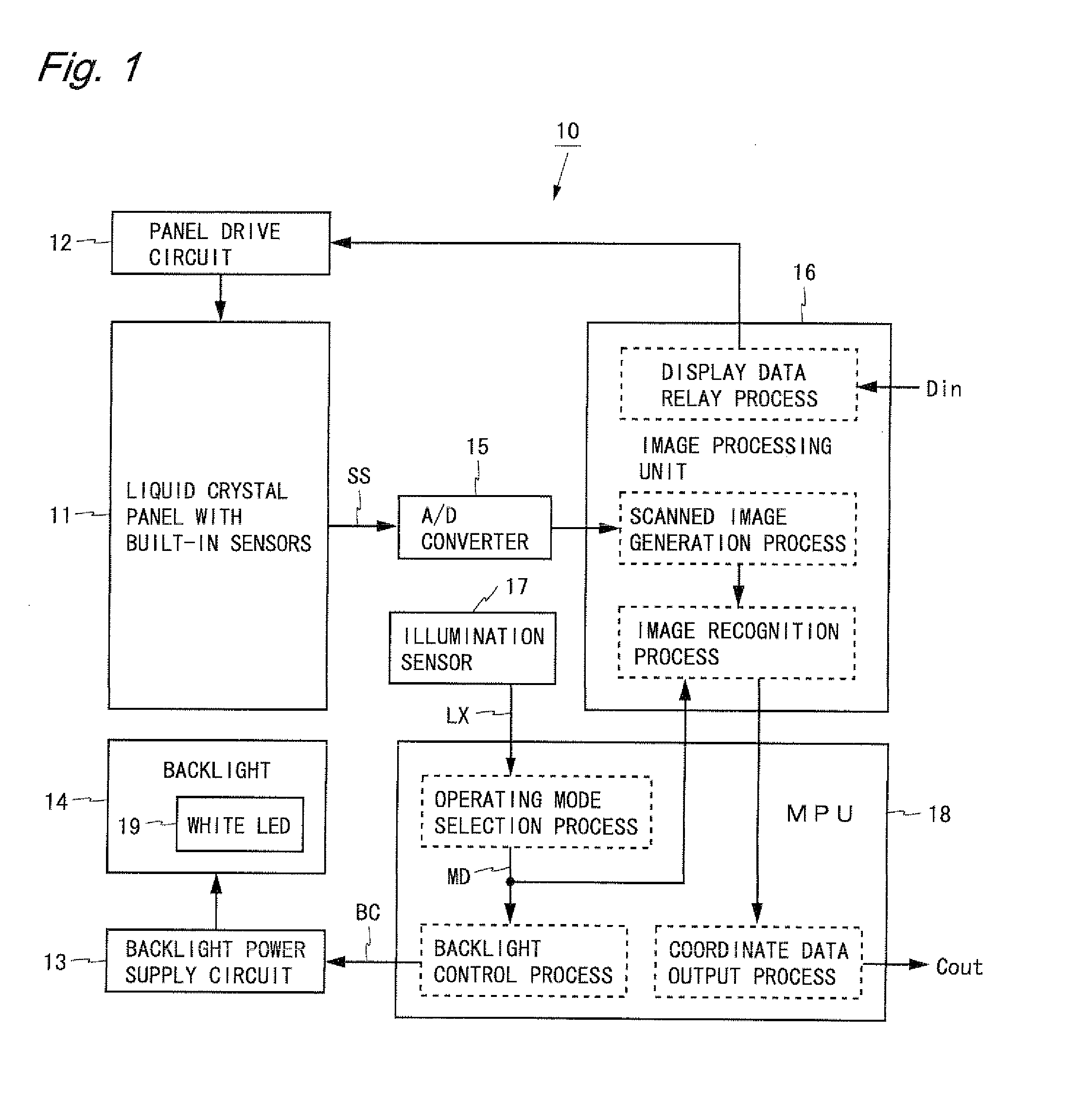
[0069]FIG. 1 is a block diagram showing a configuration of a liquid crystal display device according to a first embodiment of the present invention. A liquid crystal display device 10 shown in FIG. 1 includes a liquid crystal panel with built-in sensors 11, a panel drive circuit 12, a backlight power supply circuit 13, a backlight 14, an A / D converter 15, an image processing unit 16, an illumination sensor 17, and a microprocessor unit (hereinafter, referred to as the MPU) 18.

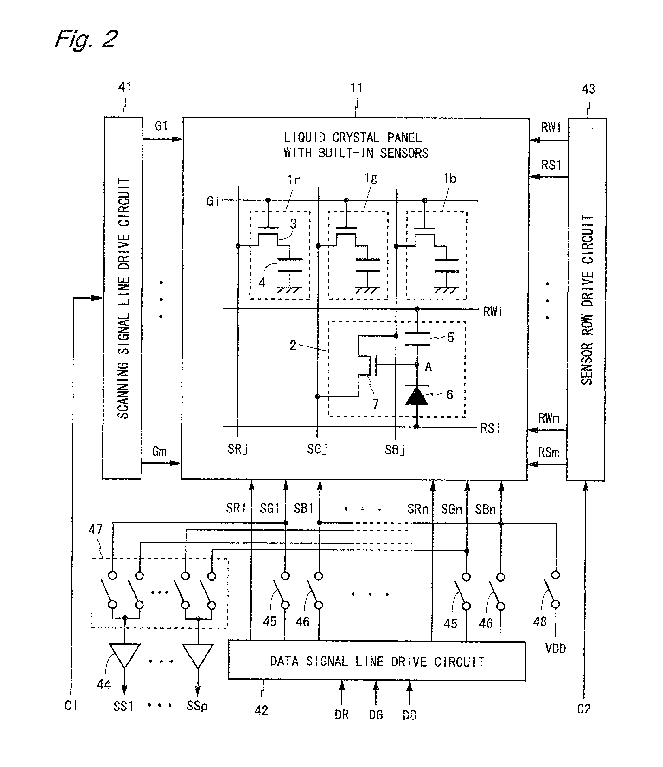
[0070]The liquid crystal panel with built-in sensors 11 (hereinafter, referred to as the liquid crystal panel 11) includes a plurality of pixel circuits and a plurality of optical sensors which are arranged two-dimensionally (details will be described later). Display data Din is inputted to the liquid crystal display device 10 from an external source. The inputted display data Din is supplied to the panel drive circuit 12 via the image processing unit 16. The panel drive circuit 12 writes voltag...

Example

Second Embodiment

[0108]FIG. 9 is a block diagram showing a configuration of a liquid crystal display device according to a second embodiment of the present invention. A liquid crystal display device 20 shown in FIG. 9 is such that in the liquid crystal display device 10 according to the first embodiment (FIG. 1), the backlight power supply circuit 13, the backlight 14, and the MPU 18 are replaced by a backlight power supply circuit 23, a backlight 24, and an MPU 28, respectively. Of the components in the present embodiment, the same components as those in the first embodiment are denoted by the same reference numerals and description thereof is omitted.

[0109]The backlight 24 includes a plurality of red LEDs 29r, a plurality of green LEDs 29g, and a plurality of blue LEDs 29. The three types of LEDs 29r, 29g, and 29b are controlled to be turned on in turn for a predetermined period of time during one frame time. The backlight power supply circuit 23 individually switches whether to s...

Example

Third Embodiment

[0115]FIG. 12 is a block diagram showing a configuration of a liquid crystal display device according to a third embodiment of the present invention. A liquid crystal display device 30 shown in FIG. 12 is such that the illumination sensor 17 is removed from the liquid crystal display device 10 according to the first embodiment (FIG. 1) and the image processing unit 16 and the MPU 18 are replaced by an image processing unit 36 and an MPU 38, respectively. Of the components in the present embodiment, the same components as those in the first embodiment are denoted by the same reference numerals and description thereof is omitted.

[0116]Display data Din inputted to the liquid crystal display device 30 is supplied to a panel drive circuit 12 via the image processing unit 36. The image processing unit 36 stores a portion of the display data Din for one frame, obtains a rate of blue components contained in the portion of the display data Din for one frame (hereinafter, refe...


PUM


Abstract

The present invention relates to a display device that has a plurality of optical sensors provided in a display panel and that can be operated by touching a screen with a finger or pen. A liquid crystal panel with built-in sensors (11) includes a plurality of pixel circuits (1) and a plurality of optical sensors (2) which are arranged two-dimensionally. An MPU (18) selects either a mode that detects a shadow image of an object or a mode that detects a reflection image of the object, based on an illumination of outside light. One frame time is divided into a display period and a sensing period. A backlight (14) is controlled to be turned on during the display period in the shadow image mode and during the sensing period in the reflection image mode, and to be turned off during the sensing period in the shadow image mode and during the display period in the reflection image mode. According to the present invention, the detection accuracy for a touch position is increased while the power consumption of the backlight is suppressed.

Description

TECHNICAL FIELD[0001]The present invention relates to a display device and more particularly to a display device having a plurality of optical sensors provided in a display panel.BACKGROUND ART[0002]In recent years, electronic devices that can be operated by touching a screen with a finger, a pen, etc., have proliferated. In addition, for a method of detecting a touch position on a display screen, a method is known in which a plurality of optical sensors are provided in a display panel and a shadow image which is created when a finger or the like approaches a screen is detected using the optical sensors.[0003]In relation to this, Patent Document 1 describes a display device in which a backlight is turned on during a display period for displaying display data on a display unit and the backlight is turned off during a sensing period during which sensor outputs from sensor units are read. According to the display device, the influence of backlight light upon detecting a shadow image is...

Claims


Application Information

Patent Timeline
IPC IPC(8): G09G5/10
CPCG02F1/13338G02F2001/13312G06F1/3203G06F1/3262G09G2360/144G06F3/042G09G3/3406G09G2330/021G06F3/0412G02F1/13312
Inventor FUJIOKA, AKIZUMIKUBOTA, AKINORI
Owner SHARP KK
Why Eureka
Try Eureka