

Optical device, electronic device, and method of manufacturing the same
- Summary
- Abstract
- Description
- Claims
- Application Information
AI Technical Summary
Benefits of technology
Problems solved by technology
Method used
Image

Examples
embodiment 1
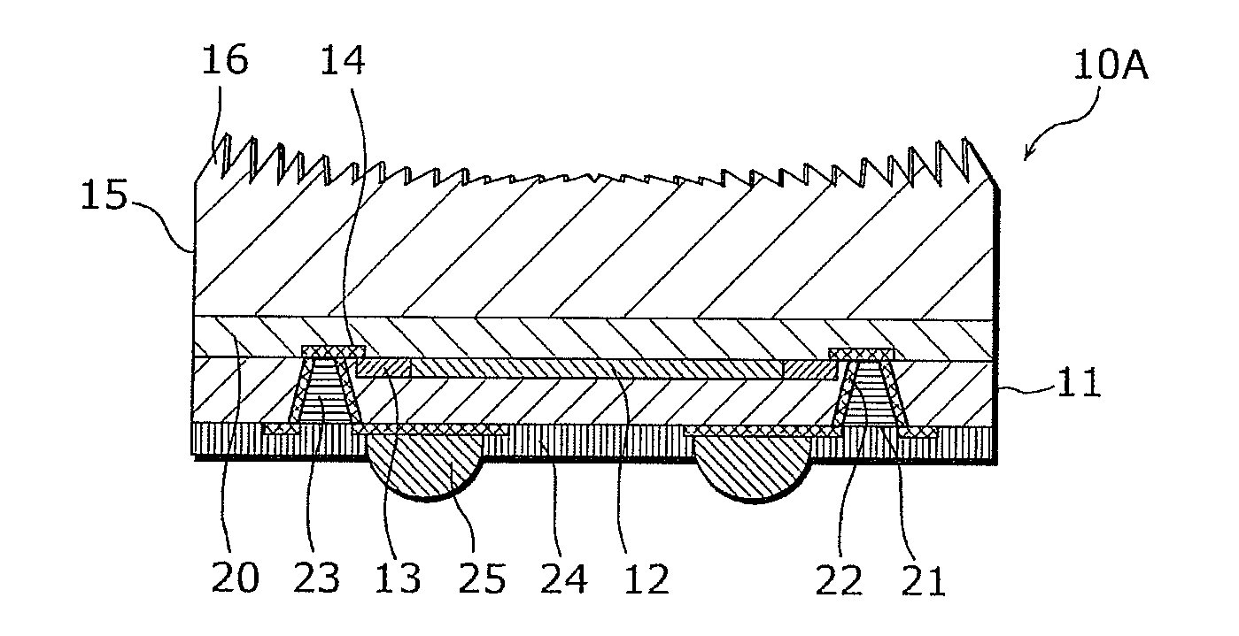
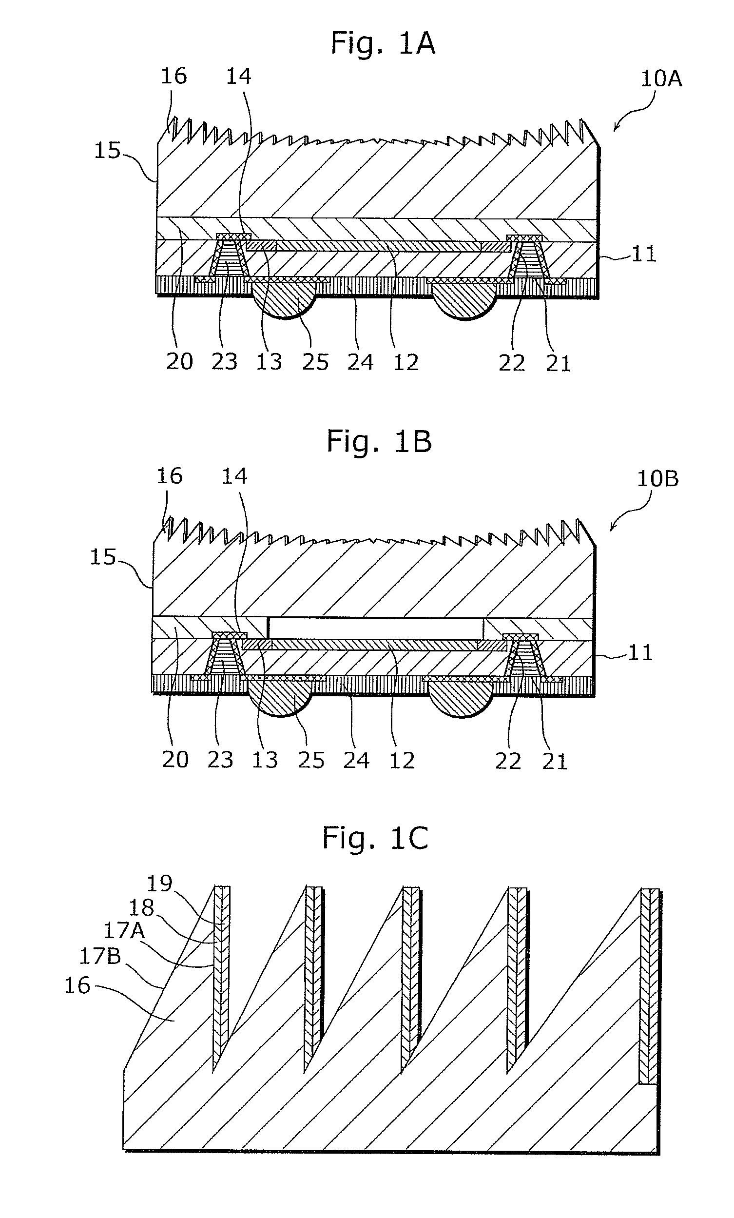
[0045]Exemplary optical devices 10A and 10B according to Embodiment 1 of the present invention are described below with reference to FIG. 1A to FIG. 1C. FIG. 1A is a cross-sectional view showing a structure of the optical device 10A according to Embodiment 1 of the present invention. FIG. 1B is a cross-sectional view showing a structure of the optical device 10B that is a variation of the optical device 10A. FIG. 1C is an enlarged view of the serrated part 16 provided in each of the optical devices 10A and 10B.
[0046]As shown in FIG. 1A, the optical device 10A includes: a semiconductor device 11; a light receiving part 12 formed on the surface (hereinafter referred to as “main surface”) of the semiconductor device 11; a peripheral circuit region 13 formed in the periphery of the light receiving part 12 and, for example, processes a signal from the light receiving part 12; an electrode region 14 formed partially using a metal thin film including Al, Cu, or the like; and a transparent ...
embodiment 2
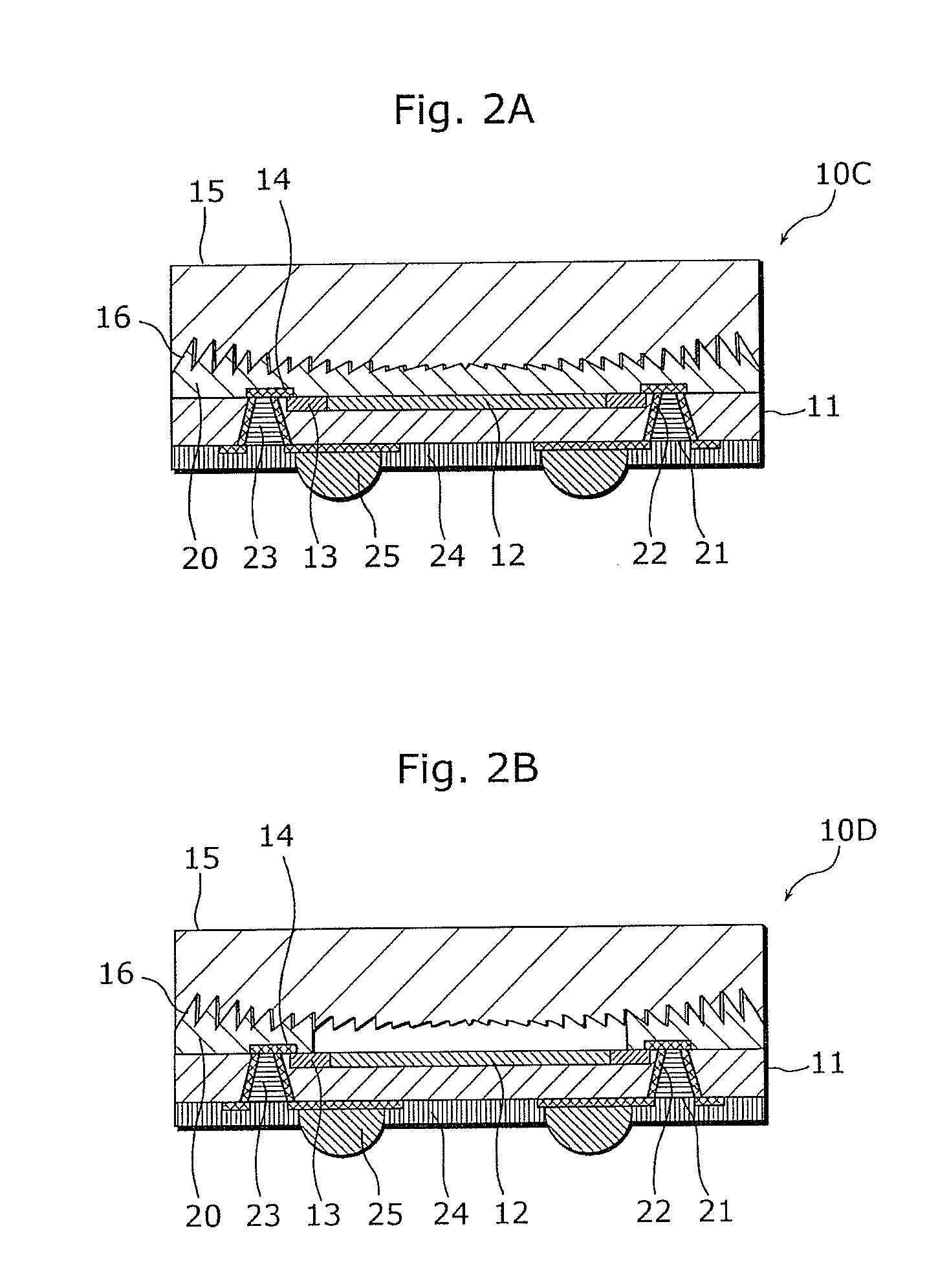
[0071]Optical devices 10C and 10D according to Embodiment 2 of the present invention are described below with reference to FIG. 2A and FIG. 2B. FIG. 2A is a cross-sectional view showing a structure of the optical device 10C according to Embodiment 2 of the present invention. FIG. 2B is a cross-sectional view showing a structure of an optical device 10D that is a variation of the optical device 10C.
[0072]As shown in FIG. 2A and FIG. 2B, the optical devices 10C and 10D are different from the optical devices 10A and 10B in Embodiment 1 in including a serrated part 16 on a surface that is of the transparent board 15 and faces the semiconductor device 11. Thus, the difference from the earlier-described embodiment is focused in the following descriptions. The structural elements common in FIG. 1A to FIG. 2B are assigned with the same reference signs, and the descriptions thereof are not repeated.
[0073]As shown in FIG. 2A, the optical device 10C according to Embodiment 2 includes the serra...
embodiment 3
[0083]Optical devices 10E and 10F according to Embodiment 3 of the present invention are described below with reference to FIG. 3A and FIG. 3B. FIG. 3A is a cross-sectional view showing a structure of the optical device 10E according to Embodiment 3 of the present invention. FIG. 3B is a cross-sectional view showing a structure of an optical device 10F that is a variation of the optical device 10E.
[0084]As shown in FIG. 3A and FIG. 3B, the optical devices 10E and 10F are different from the optical device 10A in Embodiment 1 in including a serrated part 16 on each of the upper surface and the lower surface of the transparent board 15. Thus, the difference from each of the earlier-described embodiments is focused in the following descriptions. The structural elements common in FIG. 1A to FIG. 3B are assigned with the same reference signs, and the descriptions thereof are not repeated.
[0085]As shown in FIG. 3A, the optical device 10E according to Embodiment 3 includes a serrated part 1...
PUM
 Abstract
Description
Claims
Application Information