Architecture of multi-power mode serial interface
Inactive Publication Date: 2011-06-23
IND TECH RES INST
4 Cites 13 Cited by
AI-Extracted Technical Summary
Problems solved by technology
Because USB transmission interface consumes much power, there are many examples that USB interface consumes mo...
Method used
(1) In LS/FS mode, the topology of serial interface architecture 200 is the same as standard USB, and the voltage source of serial interface architecture 200 may be lower, such as, 1.2-3.3 volts, so as to reduce power-consumption.
In summary, the disclosed embodiments provide a serial interface architecture. The serial interface architecture can be realized in a transceiver of a USB host and/or device. The transceiver can operate in many conditions, at least, including different wire lengths or transmission rates between USB host and USB device, and configurable or programmable voltage or current supplies to reduce the overall power consumption of the USB host and USB device.
The above exemplars show that the transceiver realized by the disclos...
Benefits of technology
In an exemplary embodiment, the architecture of multi-power mode serial interface comprises two I/O ports, and a driver and receiver circuit. In the driver and receiver circuit, at least a multi-mode driver generates a group of signals with different currents or voltages to drive the two I/O ports, according to control signals of different transmission modes. A multi-mode terminator circuit provides different terminal impedances, accordin...
Abstract
In one embodiment of an architecture of multi-power mode serial interface, the architecture comprises two I/O ports, and a driver and receiver circuit. In the driver and receiver circuit, at least a multi-mode driver generates a group of signals with different currents or voltages to drive the two I/O ports, according to control signals of different transmission modes. A multi-mode terminator circuit provides different terminal impedances, according to control signals of different transmission modes. At least a receiver receives signals from the two I/O ports and shunt from the multi-mode terminator circuit. Wherein, the different transmission modes at least include a USB compatible mode.
Application Domain
Modulated-carrier systemsEnergy efficient computing +2
Technology Topic
VIT signalsTransfer mode +7
Image
Examples
- Experimental program(1)
Example
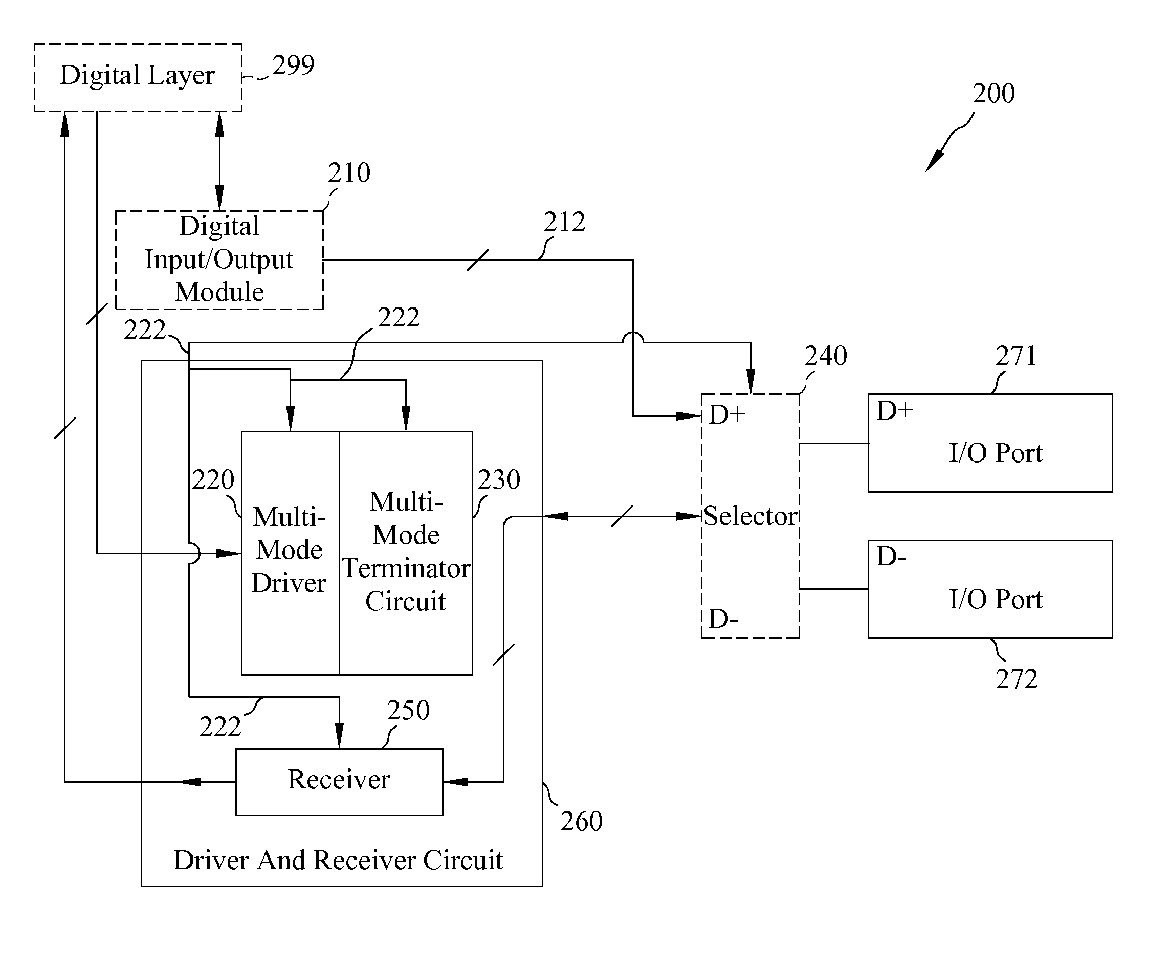
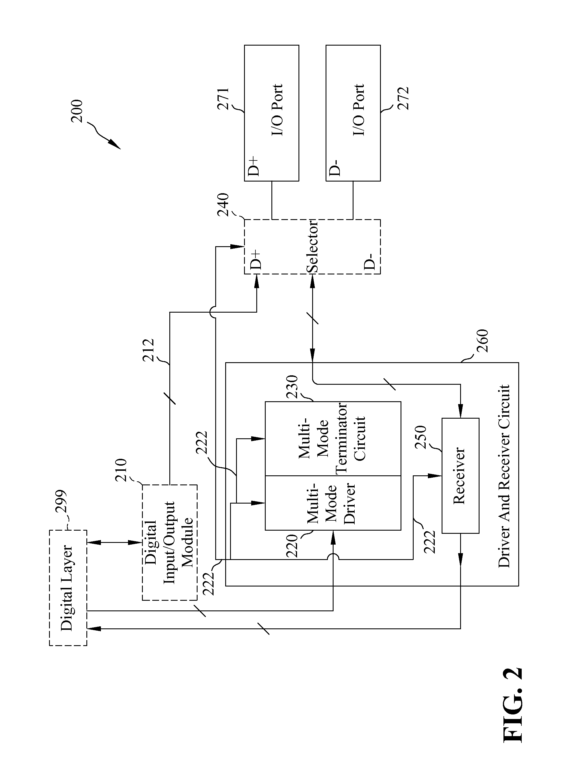
The disclosed exemplary embodiments establish a serial interface architecture in USB applications, with configurable or programmable voltage or current source and terminator circuit, and is compatible with the original USB connector as well as applicable to the USB standard cable length in the application of removable devices. In the situation of the cable length of mobile device application, a low-power mode operation may be used to achieve the requirement of energy saving for mobile devices.
The serial interface architecture may operate in many scenarios, at least including, connection wire of different lengths or different data transfer rates between the USB host and the USB device, and configurable or programmable voltage or current source so that the power consumption of the USB host and the USB device is optimized.
FIG. 2 shows an exemplary schematic view of a serial interface architecture, consistent with certain disclosed embodiments. In FIG. 2, serial interface architecture 200 comprises two I/O ports 271, 272, and a driver and receiver circuit 260. Driver and receiver circuit 260 further includes at least a multi-mode differential driver 220, a multi-mode terminator circuit 230 and at least a receiver 250.
According to control signals 222 of different transmission modes, at least a multi-mode differential driver 220 uses different current or voltage to generate a set of signals to drive two I/O ports 271, 272. At least a multi-mode driver 220 may use a differential mode for data transmission or receiving. The different transmission modes at least include a USB compatible mode.
According to control signals 22 of different transmission modes, multi-mode terminator circuit 230 provides different terminal impedances. The different terminal impedances may include adjustable output serial impedance, or adjustable input parallel terminal impedances. Multi-mode terminator circuit 230 is electrically connected to at least a multi-mode driver 220. At least a multi-mode driver 220 and multi-mode terminator circuit 230 may also be realized with a single integrated circuit.
When driver 220 transmits signals, multi-mode terminator circuit 230 may adjust the output serial impedance and suppress reflection signal according to different cable lengths and different transmission rates.
At least a receiver 250 receives signals from two I/O ports 271, 272. When receiving signals, multi-mode terminator circuit 230 may adjust the output serial impedance and suppress reflection signal according to the different cable lengths and different transmission rates. Two I/O ports 271, 272 are both electrically connected to multi-mode terminator circuit 230 and at least a receiver 250.
Serial interface architecture 200 may further include a digital I/O module 210 and at least a selector 240. Digital I/O module 210 is electrically connected to a digital layer 299 of a USB controller, and has a plurality of digital Inputs/Outputs (I/Os) 212. According to control signals 222 of different transmission modes, at least a selector 240 selects whether two I/O ports 271, 272 should be connected to driver and receiving circuit 260 or to the plurality of digital I/Os 212. The plurality of digital I/Os 212 is electrically connected to at least a selector 240. Digital I/O module 210 may also use a differential mode for data transmission and receiving. Two I/O ports 271, 272 uses a digital plus signal D+ or a digital minus signal D− for input/output.
Digital I/O 212 may have two digital signal outputs, including a digital single end data signal and a digital end clock signal, or two digital differential data signals.
In the exemplary embodiments, serial interface architecture 200 may provide three different operation modes for USB compatible data transmission: high speed (HS), full speed (FS) and low speed (LS). The definitions of HS, FS and LS data transmission rates are the same as the standard USB. In other words, 480 MHz, 12 MHz, 1.5 MHz are defined as HS, FS and LS transmission rates. Serial interface architecture 200 can further provide operation modes of different transmission rates.
Serial interface architecture 200 is compatible with a transceiver of a USB host controller/system or a USB device controller/system. The transceiver may be configured to a multi-power mode transceiver. Before a normal USB transaction processing starts, serial interface architecture 200 must determine the mode configuration according to the operation of the USB host and USB device. The operation of the USB host and the USB device is determined by the wire length or data transmission rate between the USB host and the USB device.
As aforementioned, serial interface architecture 200 can provide the USB compatible modes for three operation modes of HS, FS and LS data transmission rates. The following describes the decision of the mode configuration, wherein the general standard USB is, such as, USB 2.0.
(1) In LS/FS mode, the topology of serial interface architecture 200 is the same as standard USB, and the voltage source of serial interface architecture 200 may be lower, such as, 1.2-3.3 volts, so as to reduce power-consumption.
(2) In LS/FS mode, the host selects a set of frequencies at which both the host and the device may operate well from a set of pre-defined frequencies, such as, 1.5/12 MHz or other operating frequencies with spectrum within 1.5 MHz-12 MHz, the host-defined value as 12 MHz, where the data transmission rate can vary between 1.5 MHz and 12 Mhz. The signal quality depends on the wire length between USB host transceiver and USB device transceiver.
(3) In LS/FS mode, when establishing connection, the deviated speed can be defined through the application requirements or test packet negotiation to evaluate the bit error rate and assure the signal quality.
(4) In HS/LS/FS mode, as long as the signal quality is acceptable, the transceiver with the disclosed serial interface architecture 200 may provide a single ended mode for data wire and clock wire to replace the digital plus signal wire D+ or digital minus signal wire D− of a standard USB. The signal quality depends on the wire length between the USB host transceiver and the USB device transceiver.
(5) In HS mode, the host selects a set of frequencies at which both the host and the device can operate well from a set of pre-defined frequencies, such as, 12/60/120/240/480 MHz or other operating frequencies with spectrum within 12 MHz-480 MHz, the host-defined value as 480 MHz, where the data transmission rate may vary between 12 MHz and 480 Mhz. when the signal quality is acceptable, the data transmission rate may vary between 480 MHz to lower than 480 MHz. The signal quality depends on the wire length between USB host transceiver and USB device transceiver.
(6) In HS mode, in comparison with the driver circuit of a standard USB, multi-mode driver 220 of serial interface architecture 200 operates in a lower current mode, and receiver 250 switches to lower power termination mode.
(7) In HS mode, when establishing connection, the deviated speed may be defined through the application requirements or test packet negotiation to evaluate the bit error rate and assure the signal quality.
(8) Single-ended signaling is a simple and common manner to send electronic signal through wire, wherein a wire carries a voltage change, and the voltage change represents a signal; the other wire is connected to a reference signal, usually, the ground.
(9) The transceiver of USB host and/or USB device, in addition to the standard USB mode, also has configurable lower power mode, including, configurable or programmable driving and termination modes, and configurable or programmable synchronous single end and/or asynchronous differential mode. The synchronous single-end is, such as, the single end data with single end clock.
(10) For varied data transmission rates, the speed can be determined by (3) and (7). This is the definition of multi-mode.
(11) For modified frequency mode, the definition can refer to (2) and (5).
As aforementioned, the disclosed serial interface architecture can be realized in a transceiver of a USB host controller transceiver or a USB device controller. Alternatively, both the host controller or the device controller include the transceiver having the serial interface architecture of the present invention, and the transceiver of the host and the transceiver of the device form symmetric circuit. The transceiver may be configured to a multi power mode. The transceiver of the USB device controller may also be designed with the digital input/output module of the above exemplary embodiment, at least a multi-mode driver, a multi-mode termination circuit, a receiver and at least a selector circuit.
FIG. 3 shows an exemplary schematic view of a working exemplar of the serial interface architecture 200, consistent with certain disclosed embodiments. In FIG. 3, digital output module 210 generates four digital signal outputs, including a digital single end data output 320, a digital single end clock output 322, a digital differential end data output 321, and a digital differential end clock output 323, wherein digital single end data output 320 and digital single end clock output 322 are provided to a first multiplexer 341, and digital differential end data output 321 and digital differential end clock output 323 are provided to a second multiplexer 342.
For HS or deviated HS mode, multi-mode high speed driver 330, via control signal 330a, uses different currents or different volts, and different output impedances to drive in current mode or voltage mode. The multi-mode low/full speed driver 340, via control signal 340a, uses different volts, and different output impedances to drive in voltage mode, and includes a first multi-PWR mode terminator 351 and a second multi-PWR mode terminator 352. Based on the default mode configuration, when receiving signals, driver 340 outputs a fixed level, such as, low level, and the terminators 351, 352 form parallel termination resistance.
When the wire length between the host transceiver and the device transceiver is short, under the circumstance of passing through a certain length of wire at a default transmission rate, as long as the signal quality is with an acceptable bit error rate (BER), the signal receiving does not have to activate parallel termination resistance formed by driver 340, and multi-PWR mode terminators 351, 352; that is, no parallel termination at all, so as to reduce the transmission power consumption.
For LS/FS or deviated LS/FS mode, multi-mode HS driver 430 is turned off. Multi-mode LS/FS driver 340, via control signal 340a, uses different voltage swings to drive according to the default mode configuration and system-provided voltage supply to assure the signal quality still has an acceptable BER after passing through a certain wire length at a default frequency.
As shown in the working exemplar of FIG. 4, multi-mode HS driver 330 and multi-mode LS/FS driver 340 may also be integrated as a unified driver circuit, that is, a multi-power mode L/F/HS driver 450. Multi-power mode L/F/HS driver 450 may include the capabilities of multi-mode HS driver 330 and multi-mode LS/FS driver 340. For HS or deviated HS mode, multi-power mode L/F/HS driver 450 can use different currents or different volts, and different impedances to drive in current mode or voltage mode. For LS/FS or deviated LS/FS mode, multi-power mode L/F/HS driver 450 will use different voltage swings to drive. Similarly, first multi-PWR terminator 351 and second multi-PWR terminator 352 may be integrated into a unified terminator circuit, such as, a multi-power mode L/F/HS terminator 430, to provide different input parallel termination resistances in different power mode.
The above exemplars show that the transceiver realized by the disclosed serial interface architecture can operate in a plurality of conditions, including different transmission wire lengths, a plurality of data rates and supply voltages, to optimize the power consumption of the USB host and device. The configurable or programmable driving mode may provide different currents in a plurality of current modes for different wire lengths at standard rates or non-standard deviated speeds. The configurable or programmable termination mode may provide different termination resistances, including infinite resistance, i.e., no parallel termination at all, for different wire lengths at standard rates or non-standard deviated speeds. The transceiver is compatible with USB device/system as well as USB host controller/system.
The serial interface architecture of the disclosed embodiments may define a port layout. The port layout may be placed at the controller end of a host transceiver or the controller end of a device transceiver. With the port layout design and FIGS. 3-4, it may be seen that the serial interface architecture of the disclosed embodiments includes multi-mode drivers and multi-mode terminators and optional digital and/or single-ended driver. The single-ended mode provides data wire and clock wire to replace the digital plus signal wire D+ and digital minus signal wire D− of the standard USB, such as, USB 2.0.
In summary, the disclosed embodiments provide a serial interface architecture. The serial interface architecture can be realized in a transceiver of a USB host and/or device. The transceiver can operate in many conditions, at least, including different wire lengths or transmission rates between USB host and USB device, and configurable or programmable voltage or current supplies to reduce the overall power consumption of the USB host and USB device.
Although the present invention has been described with reference to the exemplary embodiments, it will be understood that the invention is not limited to the details described thereof. Various substitutions and modifications have been suggested in the foregoing description, and others will occur to those of ordinary skill in the art. Therefore, all such substitutions and modifications are intended to be embraced within the scope of the invention as defined in the appended claims.
PUM


Description & Claims & Application Information
We can also present the details of the Description, Claims and Application information to help users get a comprehensive understanding of the technical details of the patent, such as background art, summary of invention, brief description of drawings, description of embodiments, and other original content. On the other hand, users can also determine the specific scope of protection of the technology through the list of claims; as well as understand the changes in the life cycle of the technology with the presentation of the patent timeline. Login to view more.