

Film formation system and film formation method
- Summary
- Abstract
- Description
- Claims
- Application Information
AI Technical Summary
Benefits of technology
Problems solved by technology
Method used
Image

Examples
Example
[0031]The following illustrative embodiments are provided to illustrate the disclosure of the present invention and its advantages, these and other advantages and effects being readily understandable by those in the art after reading the disclosure of this specification. The present invention can also be performed or applied by other embodiments. The details of the specification may be on the basis of a particular viewpoint or application, and numerous modifications and variations can be devised without departing from the spirit of the present invention.
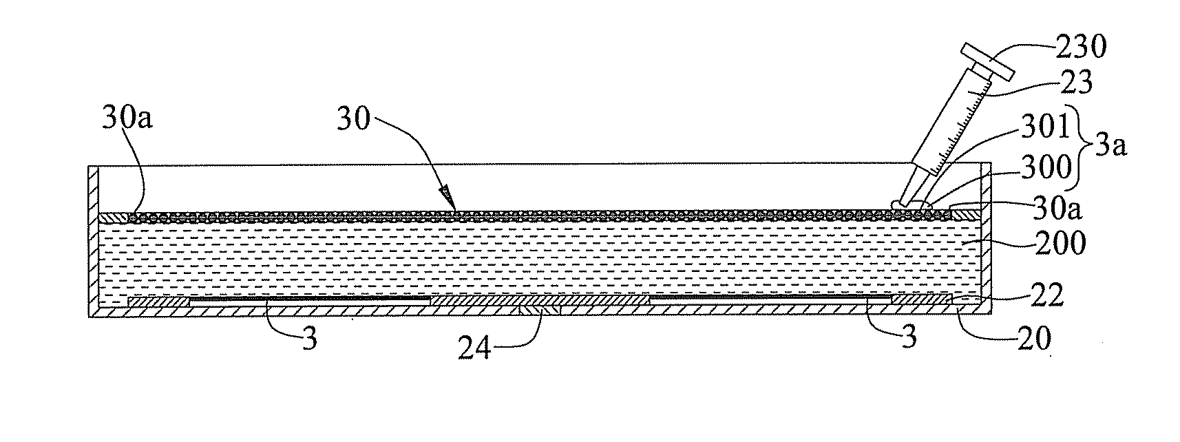
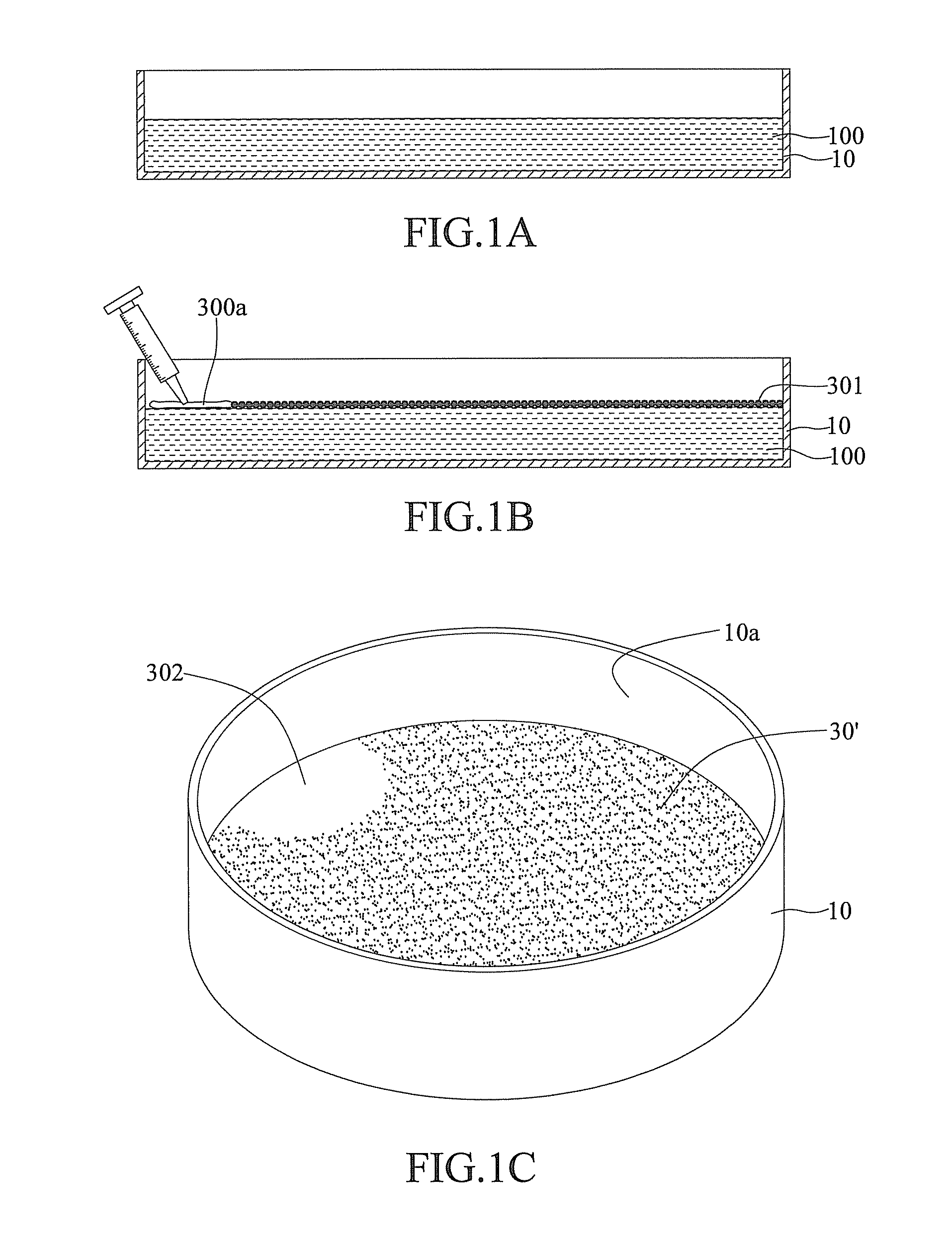
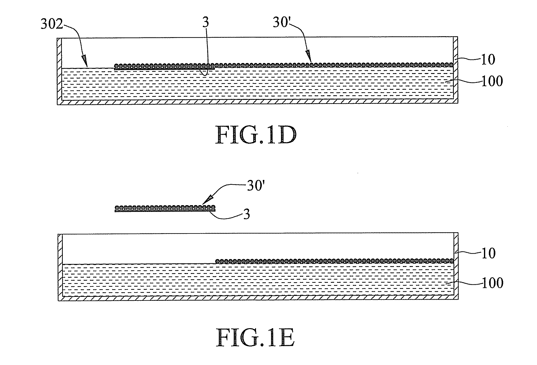
[0032]FIG. 2 shows a film formation system 2 according to an embodiment according to the present invention. Please also refer to FIGS. 3A-3E, which are cross-sectional diagrams illustrating a film formation method applied to the film formation system 2. Also, please refer to FIGS. 4A-4C, which show the film formation system 2 of other embodiments. The film of the present invention may be used as an etching mask or used for other purp...
PUM
 Abstract
Description
Claims
Application Information