Imaging module, fabricating method therefor, and imaging device

a technology of imaging module and fabricating method, which is applied in the direction of individual semiconductor device testing, semiconductor/solid-state device testing/measurement, instruments, etc., can solve the problems of polarizer without variability, difficult to arrange the polarizer so close and difficult to arrange the polarizer as close as desired to the light-receiving surface of the imaging elemen

Inactive Publication Date: 2011-07-28
RICOH KK
View PDF2 Cites 19 Cited by
  • Summary
  • Abstract
  • Description
  • Claims
  • Application Information

AI Technical Summary

Benefits of technology

[0011]It is a general object of at least one embodiment of the present invention to provide an imaging module capable of preventing foreign matter from attaching to a light-receiving surface thereof without degrading light receiving properties, a fabricating method for such an imaging module, and an imaging device having the imaging module that substantially eliminate one or more problems caused by the limitations and disadvantages of the related art.

Problems solved by technology

However, with the configuration of the related art semiconductor imaging device disclosed in Patent Document 1, it may be difficult to arrange the polarizer so close to the light-receiving surface of the imaging element, and to maintain the constant distance between the light-receiving surface of the imaging element and the polarizer without variability.
Thus, it may be difficult to arrange the polarizer as close as desired to the light-receiving surface of the imaging element.
However, the distance between the light-receiving surface of the imaging element and the polarizer may vary and thus not be constant due to inability to arrange the polarizer based on the light-receiving surface of the imaging element as the origin if the polarizer is arranged away from the light-receiving surface of the imaging element.
This may interfere with incident light received on the light-receiving surface of the CCD 302.
Thus, the adhesive 305 may cause optical distortion of incident light to drastically lower optical properties of the micro-lenses 304.

Method used


Image

  • Imaging module, fabricating method therefor, and imaging device
  • Imaging module, fabricating method therefor, and imaging device
  • Imaging module, fabricating method therefor, and imaging device

Examples


Embodiment Construction

[0030]In the following, embodiments of the present invention will be described with reference to the accompanying drawings.

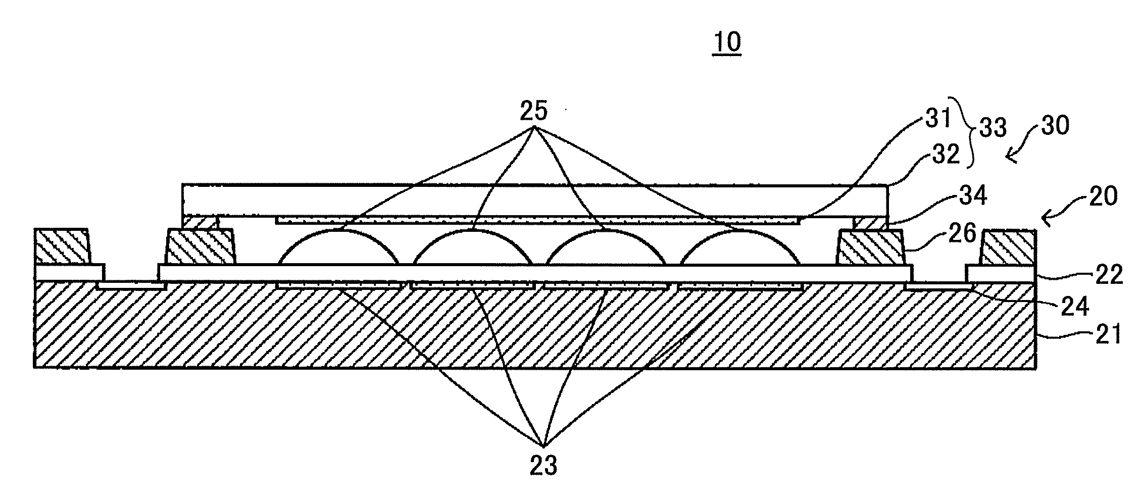
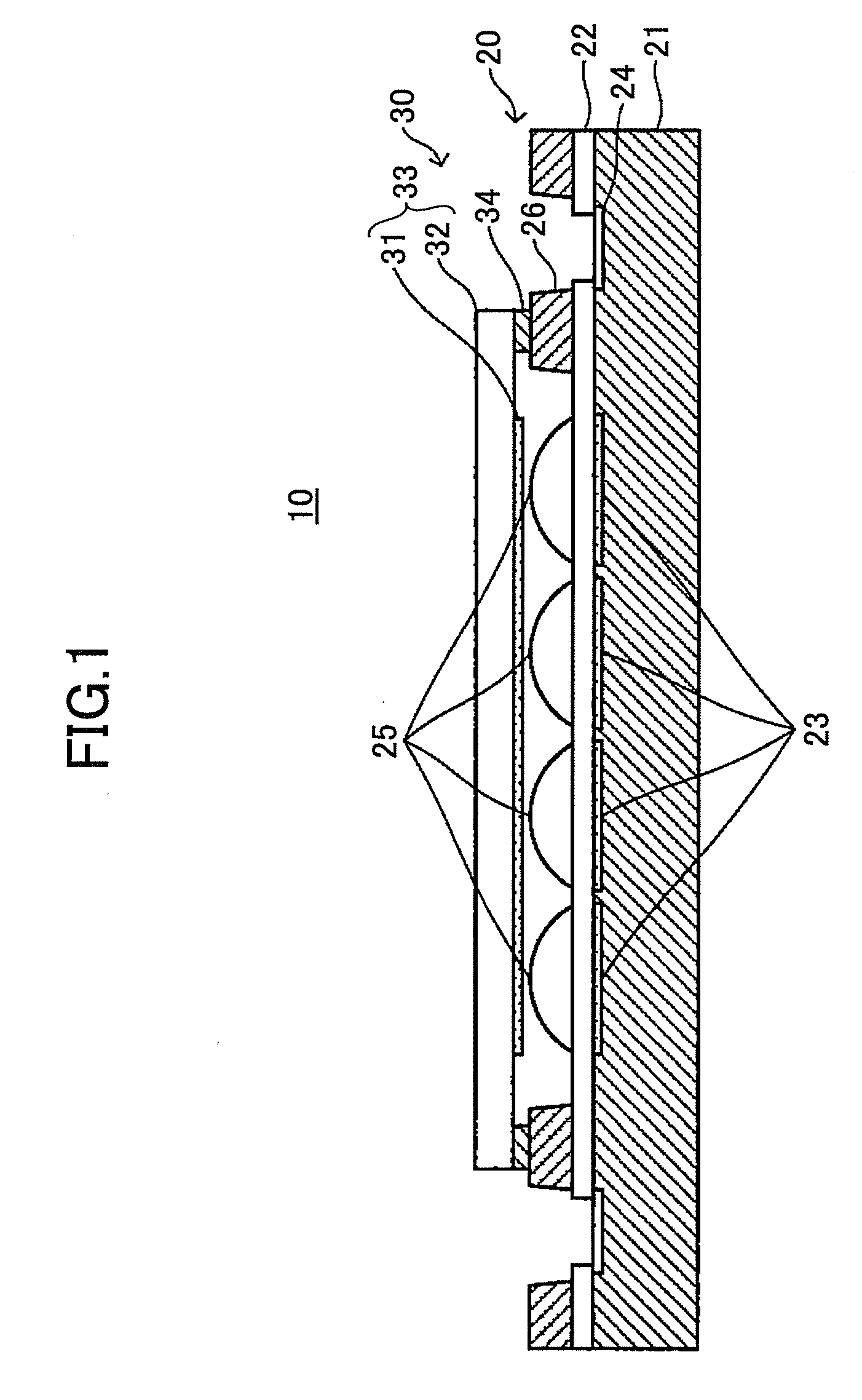
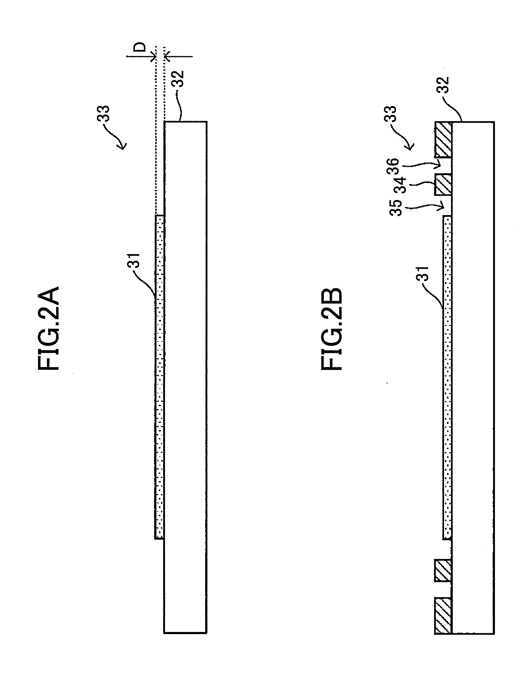
[0031]FIG. 1 is a cross-sectional diagram illustrating a configuration of an imaging module according to an embodiment. As illustrated in FIG. 1, an imaging module 10 according to the embodiment includes an imaging chip 20 and a polarizing glass chip 30. The imaging chip 20 includes a semiconductor substrate 21, an inorganic insulator film 22 made of an oxide film such as a SiO2 film, imaging elements 23, electrode pads 24, micro-lenses 25, and a structural film 26. The imaging elements 23 are configured to convert incident light into electric signals and are provided between the semiconductor substrate 21 and the inorganic insulator film 22. The electric pads 24 are nodes configured to supply the electric signals from the imaging elements 23 to an external circuit and are arranged near the outer periphery of a collection of light-receiving surfaces of the imagi...


PUM


Abstract

An imaging module includes an imaging chip including a micro-lens guiding incident light and an imaging element in a semiconductor substrate and converting the incident light into an electric signal, and a polarizing glass chip including a polarizing filter glass having a polarizer determining a polarization direction of the incident light arranged on a transparent substrate such that the polarizer faces the micro-lens and a spacer member connected to the polarizing filter glass to adjust a gap between the polarizer and the micro-lens of the imaging chip. In the imaging module, a melt-bonding surface of the spacer member is melt-bonded to the semiconductor substrate such that the polarizer of the polarizing glass chip and the micro-lens of the imaging chip are arranged close to each other via the gap, and the imaging element and the micro-lens of the imaging chip are sealed by the polarizing glass chip.

Description

BACKGROUND OF THE INVENTION[0001]1. Field of the Invention[0002]The invention generally relates to an imaging module capable of preventing foreign matter from attaching to a light-receiving surface thereof without degrading light receiving properties, a fabricating method for such an imaging module, and an imaging device having the imaging module.[0003]2. Description of the Related Art[0004]There are increasing demands on high density implementation of semiconductor components while growing demands on reduction in size and weight on electronic devices. Specifically, there are increasing demands on high integration of semiconductor imaging devices owing to advances in microfabrication technologies. In addition, various fabrication methods have been proposed for fabricating light-weight semiconductor imaging devices at low cost.[0005]For example, a related art semiconductor imaging device includes a semiconductor imaging element having a light-receiving portion and a micro-lens config...

Claims


Application Information

Patent Timeline
Patent Type & Authority Applications(United States)
IPC IPC(8): H01L31/0232H01L21/66
CPCH01L27/14618H01L2924/0002H01L2924/00
Inventor MINEGISHI, DAIKISATOH, YASUHIROMOCHIZUKI, EIJIFUJISHIMA, MASAYUKIMIURA, HIROSHI
Owner RICOH KK
Why Eureka
Try Eureka