Semiconductor apparatus

a semiconductor and apparatus technology, applied in the field of semiconductor apparatuses, can solve the problems of hardly showing the same performance characteristics, affecting the economic efficiency of semiconductor apparatuses, and affecting the so as to improve the economic efficiency and thereby price competitiveness of semiconductor apparatuses

Inactive Publication Date: 2011-08-04
SK HYNIX INC
View PDF7 Cites 12 Cited by
  • Summary
  • Abstract
  • Description
  • Claims
  • Application Information

AI Technical Summary

Benefits of technology

[0011]Accordingly, various exemplary aspects of the invention may provide semiconductor apparatuses and / or methods that may is improve the economic efficiency and thereby price competitiveness of a semiconductor apparatus. In particular, a semiconductor apparatus capable of correcting skews of a plurality of stacked chips constituting a single semiconductor apparatus is described herein.

Problems solved by technology

Because the stacked chips have different characteristics due to variations in PVT (process, voltage and temperature), however, they can hardly show the same performance characteristics.
More specifically, the respective chips have skews due to their different PVT properties.
Thus, a skew may result from the difference in data output timing between a chip with a high operational speed and one with a low operational speed.

Method used


Image

  • Semiconductor apparatus
  • Semiconductor apparatus
  • Semiconductor apparatus

Examples


Embodiment Construction

[0024]Reference will now be made in detail to the exemplary embodiments consistent with the present disclosure, examples of which are illustrated in the accompanying drawings. Wherever possible, the same reference characters will be used throughout the drawings to refer to the same or like parts.

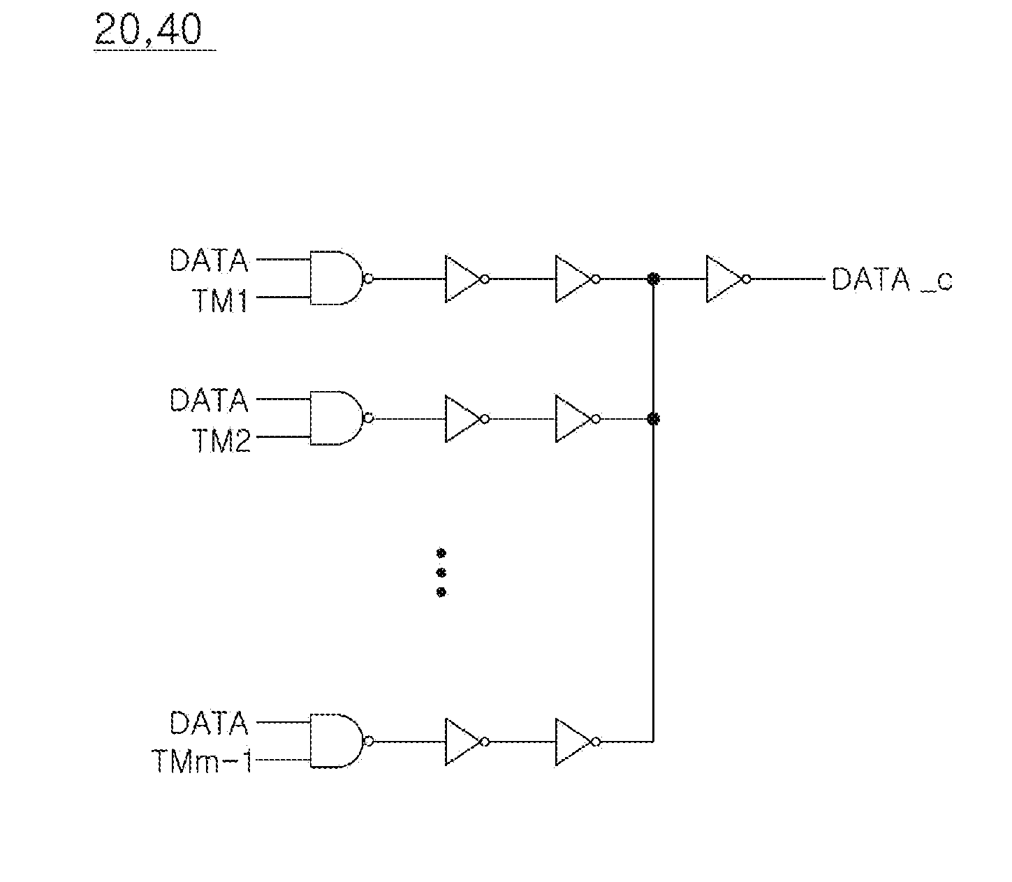
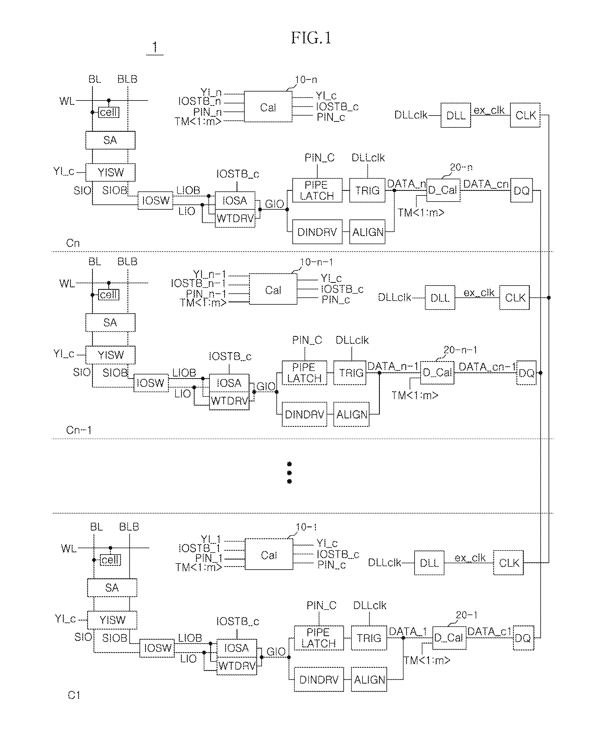
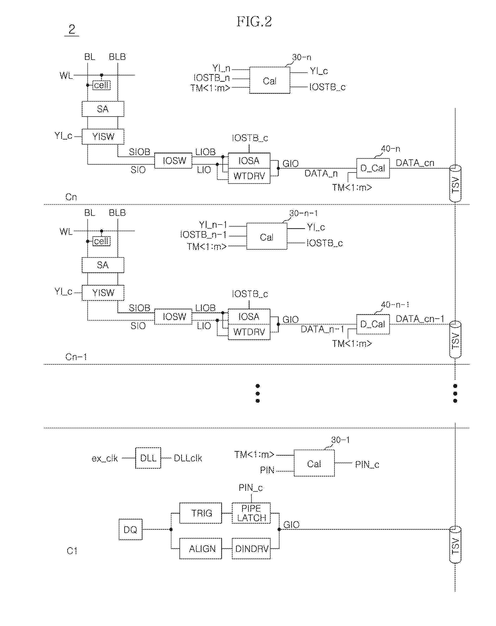
[0025]FIG. 1 schematically illustrates an exemplary configuration of a semiconductor apparatus consistent with various exemplary aspects of the invention. Referring to FIG. 1, a semiconductor apparatus 1 is configured as a 3D semiconductor apparatus in which a plurality of structurally similar chips are stacked. The semiconductor apparatus 1 includes first to nth chips C1-Cn. The first to nth chips C1-Cn may operate as a single semiconductor apparatus because the data pads DQ thereof are connected through wires such as metal wires. An external clock ex_clk is inputted through clock pads CLK which are provided in the respective chips through wires.

[0026]In FIG. 1, the first to nth chips C1-Cn...


PUM


Abstract

A semiconductor apparatus has a plurality of chips stacked therein, and generation timing of read control signals for controlling read operations of the plurality of stacked chips is controlled such that times after a read command is applied to when data are outputted from respective chips are made to substantially correspond to one another.

Description

CROSS-REFERENCES TO RELATED APPLICATION[0001]The present application claims priority under 35 U.S.C. §119(a) to Korean Patent Application No. 10-2010-0008635, filed on Jan. 29, 2010, in the Korean Intellectual Property Office, which is incorporated herein by reference in its entirety as if set forth in full.BACKGROUND[0002]1. Technical Field[0003]Various exemplary aspects of the present invention relate to a semiconductor apparatus. In particular, certain exemplary aspects relate to a three-dimensional semiconductor apparatus.[0004]2. Related Art[0005]In order to increase the degree of integration of a semiconductor apparatus, a 3D (three-dimensional) semiconductor apparatus has been developed. The 3-D semiconductor apparatus includes a plurality of chips stacked for placement in a single package. The resultant structure is then packaged. The 3D semiconductor apparatus may achieve a maximum degree of integration in the same space by vertically stacking two or more chips.[0006]The 3D...

Claims


Application Information

Patent Timeline
Patent Type & Authority Applications(United States)
IPC IPC(8): H03K19/173
CPCH03K19/173G11C29/028G11C7/1066H01L25/0657G11C29/50012G11C29/023G11C7/1051
Inventor BYEON, SANG JINLEE, JAE JIN
Owner SK HYNIX INC
Why Eureka
Try Eureka