Semiconductor apparatus and probe test method thereof

a technology of semiconductor devices and probes, which is applied in the direction of individual semiconductor device testing, semiconductor/solid-state device testing/measurement, instruments, etc., can solve the problems of increasing the total number of chips on the wafer, the logic circuit of the probe test logic circuit cannot be easily removed, and the inability to perform the probe test. the effect of economic efficiency and thereby price competitiveness of the semiconductor apparatus

Inactive Publication Date: 2011-06-30
SK HYNIX INC
View PDF17 Cites 8 Cited by
  • Summary
  • Abstract
  • Description
  • Claims
  • Application Information

AI Technical Summary

Benefits of technology

[0011]Accordingly, various exemplary embodiments of the invention may provide semiconductor apparatuses and / or methods that may improve the economic efficiency and thereby price competitiveness of a semiconductor apparatus. In particular, certain exemplary embodiments may provide semiconductor apparatuses and related methods that can allow a logic circuit for conducting a probe test to be removed after completing the probe test, which in turn may increase the wafer space available for placing additional number of chips.

Problems solved by technology

A probe test logic circuit for performing the probe test may be useless except when the chip is tested on the wafer.
However, since the probe test logic circuit is conventionally disposed in the peripheral region PERI where a logic circuit for ensuring the normal operation of the semiconductor apparatus and bondings of pads are located, the probe test logic circuit could not be easily removed.
However, manufacturing the slave chips according to the above-mentioned conventional methods may not permit such an increase in the total number of chips on a wafer and therefore is economically inefficient.

Method used


Image

  • Semiconductor apparatus and probe test method thereof
  • Semiconductor apparatus and probe test method thereof
  • Semiconductor apparatus and probe test method thereof

Examples


Embodiment Construction

[0025]Reference will now be made in detail to the exemplary embodiments consistent with the present disclosure, examples of which are illustrated in the accompanying drawings. Wherever possible, the same reference characters will be used throughout the drawings to refer to the same or like parts.

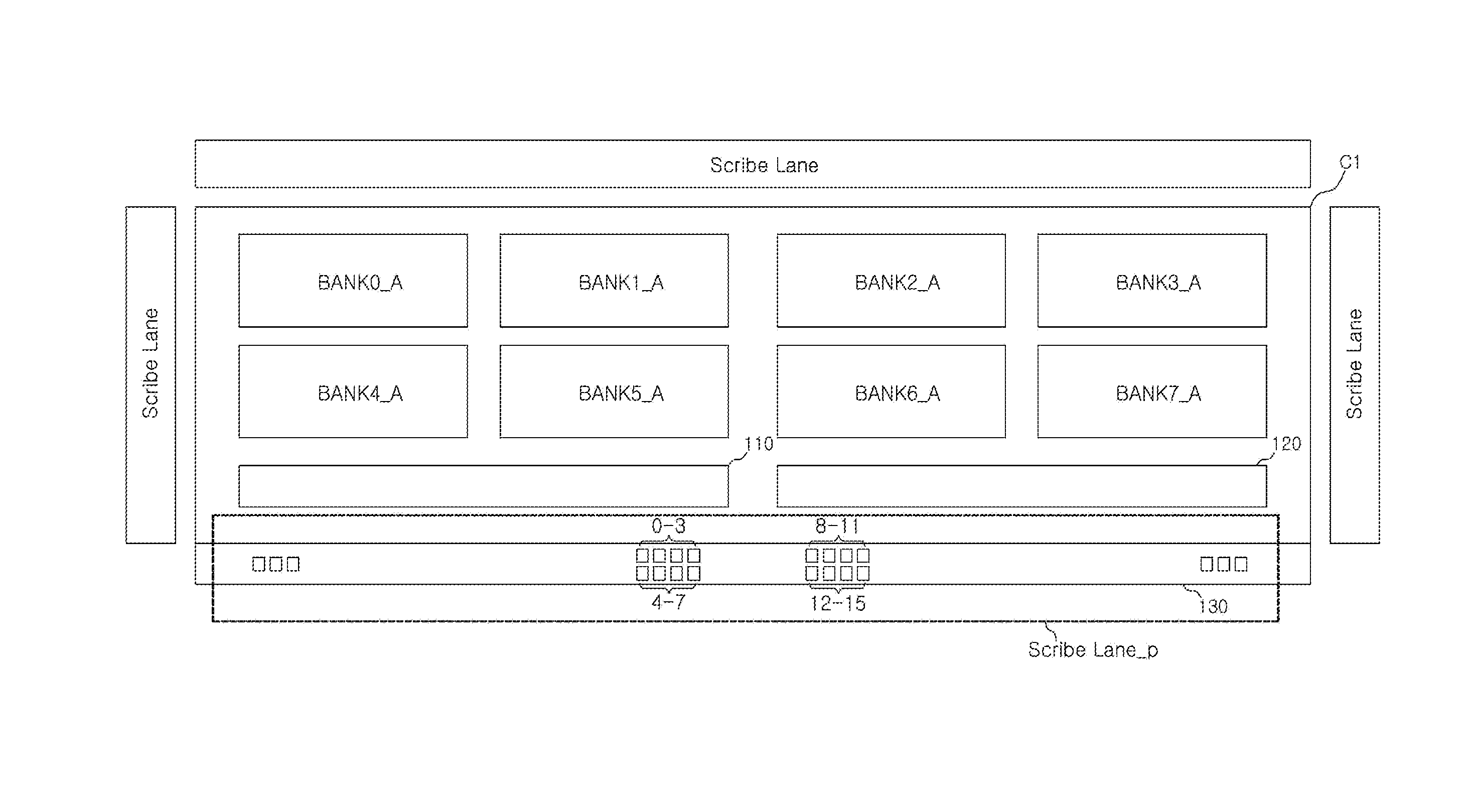
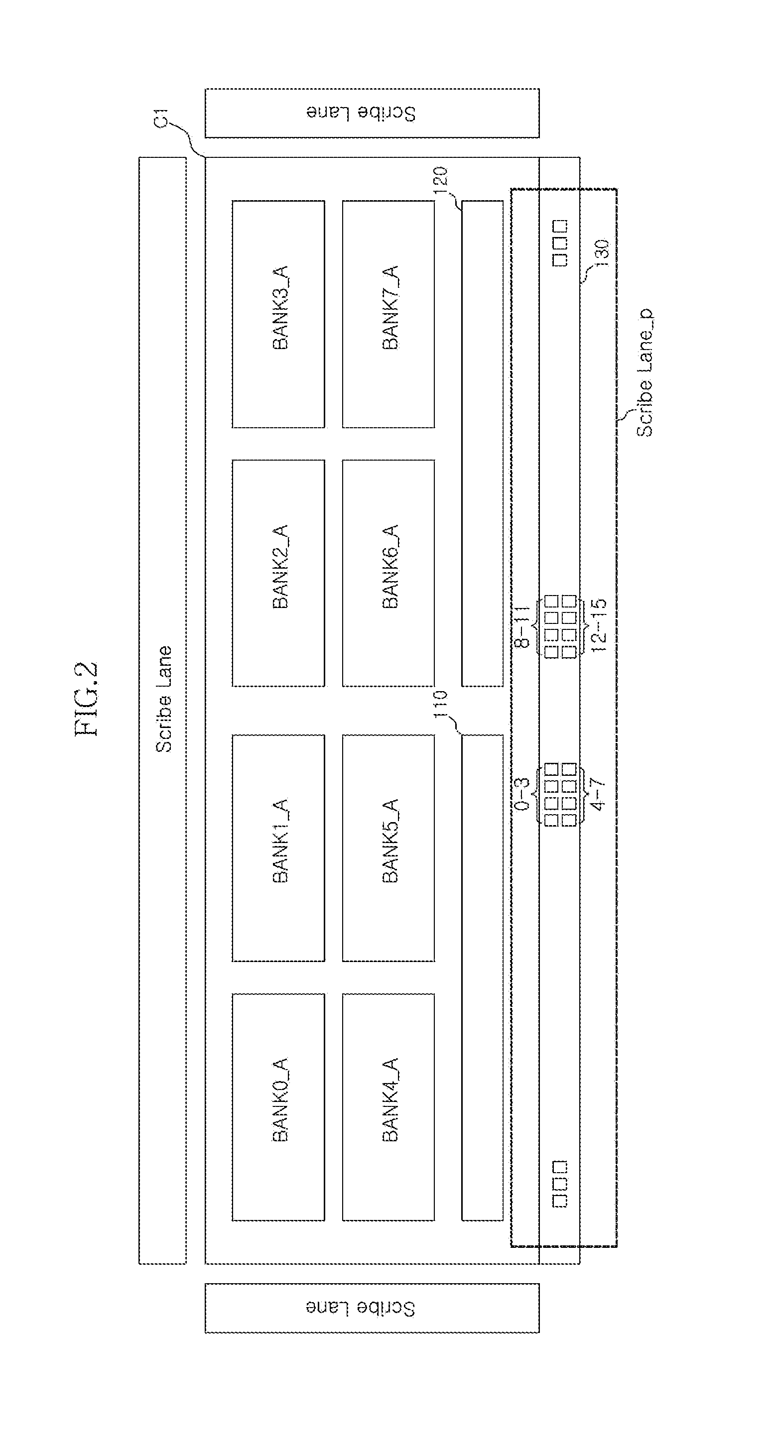
[0026]FIG. 2 schematically illustrates an exemplary layout of a semiconductor chip C1 of a semiconductor apparatus consistent with various exemplary aspect of the invention. Referring to FIG. 2, chip C1 includes a plurality of memory banks BANK0_A through BANK7_A. Chip C1 also includes chip operation logic circuits 110 and 120 associated with the operation of the memory banks BANK0_A through BANK7_A. Chip operation logic circuits 110 and 120 may be disposed laterally of the memory banks BANK0_A through BANK7_A, as shown in FIG. 2. In various exemplary embodiments, chip operation logic circuits 110 and 120 may include, but not be limited to, repair circuits for the memory banks BANK0_A throug...


PUM


Abstract

Various embodiments of a semiconductor apparatus and related methods are disclosed. In one exemplary embodiment, a semiconductor apparatus may include a chip, scribe lanes disposed around the chip, and a probe test logic circuit for conducting a probe test on the chip. The probe test logic circuit is disposed on a portion of the scribe lanes.

Description

CROSS-REFERENCES TO RELATED APPLICATION[0001]The present application claims priority under 35 U.S.C. §119(a) to Korean Patent Application No. 10-2009-0131791, filed on Dec. 28, 2009, in the Korean Intellectual Property Office, which is incorporated herein by reference in its entirety as if set forth in full.BACKGROUND[0002]1. Technical Field[0003]Various embodiments of the present invention relate to semiconductor apparatuses and related methods. In particular, certain exemplary embodiments relate to a semiconductor apparatus is and a probe test method thereof.[0004]2. Related Art[0005]A semiconductor apparatus, in particular, a memory apparatus has a memory core for storing data. Logic circuits for ensuring the normal operation of the semiconductor apparatus and for performing tests are generally disposed in a peripheral region of the memory core. The logic circuits for performing tests may include a probe test logic circuit for measuring the internal voltage levels or for performi...

Claims


Application Information

Patent Timeline
Patent Type & Authority Applications(United States)
IPC IPC(8): G01R1/06H01L21/66G01R31/26
CPCH01L22/34G11C29/006H01L2924/0002H01L2924/00H01L22/00
Inventor YUN, TAE SIKLEE, JONG CHERN
Owner SK HYNIX INC
Why Eureka
Try Eureka