Semiconductor apparatus

a semiconductor and circuit technology, applied in the field of three-dimensional semiconductor apparatuses, can solve the problems of skew in data output timing, difficult for them to perform similarly, and pvt properties create skews between the respective chips, so as to improve the economic efficiency and thereby price competitiveness of the semiconductor apparatus

Active Publication Date: 2011-08-04
SK HYNIX INC
View PDF23 Cites 7 Cited by
  • Summary
  • Abstract
  • Description
  • Claims
  • Application Information

AI Technical Summary

Benefits of technology

[0011]Accordingly, various exemplary exemplary aspects of the invention may provide semiconductor apparatuses and / or methods that may improve the economic efficiency and thereby price competitiveness of a semiconductor apparatus. In particular, a semiconductor apparatus capable of correcting skews of a plurality of stacked chips constituting a single semiconductor apparatus is described herein.

Problems solved by technology

However, because the stacked chips have different characteristics due to variations in PVT (process, voltage and temperature), it is difficult for them to perform similarly.
More specifically, the different PVT properties create skews between the respective chips.
Thus, a skew in data output timing between a chip having a high operating speed and a chip having a low operating speed may result.
In order to secure a data valid window in the existence of the skew, therefore, the operating speed of the semiconductor apparatus should be lowered, which is not desirable.

Method used


Image

  • Semiconductor apparatus
  • Semiconductor apparatus
  • Semiconductor apparatus

Examples


Embodiment Construction

[0018]Reference will now be made in detail to the exemplary embodiments consistent with the present disclosure, examples of which are illustrated with reference to the accompanying drawings. Wherever possible, the same reference characters will be used throughout the drawings to refer to the same or like parts.

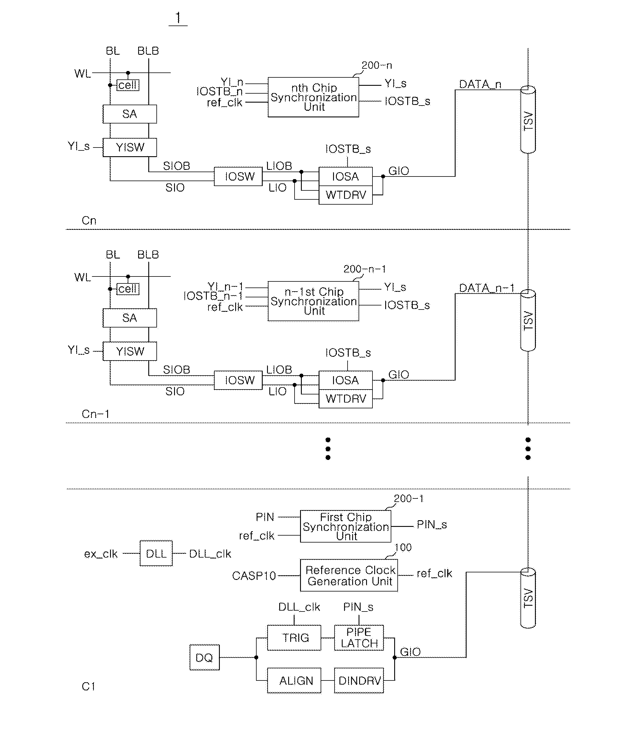
[0019]FIG. 1 is a diagram schematically illustrating the configuration of a semiconductor apparatus consistent with various exemplary aspects of the present invention. In FIG. 1, a semiconductor apparatus 1 includes first to nth chips C1-Cn. The first to nth chips C1-Cn are stacked and constitute a single semiconductor apparatus. The first to nth chips C1-Cn are connected through TSVs (through-silicon vias).

[0020]When the semiconductor apparatus uses the TSVs, data outputted from the respective chips are transmitted through the TSVs. Because each chip does not need to have data pads, data pads may be provided one chip out of the stacked chips. The chip with data pads DQ may fu...


PUM


Abstract

A semiconductor apparatus has a plurality of chips stacked therein. Read control signals for controlling read operations of the plurality of chips are synchronized with a reference clock such that the time taken from the application of a read command to the output of data for each of the plurality of chips is maintained substantially the same.

Description

CROSS-REFERENCES TO RELATED APPLICATION[0001]The present application claims priority under 35 U.S.C. §119(a) to Korean Patent Application No. 10-2010-0008636, filed on Jan. 29, 2010, in the Korean Intellectual Property Office, which is incorporated herein by reference in its entirety as if set forth in full.BACKGROUND[0002]1. Technical Field[0003]Various exemplary aspects of the present invention relate to semiconductor apparatuses and related methods. In particular, certain exemplary aspects relate to a three-dimensional semiconductor apparatus.[0004]2. Related Art[0005]In order to increase the degree of integration of a semiconductor apparatus, a 3D (three-dimensional) semiconductor apparatus has been developed. The 3D semiconductor includes a package of a plurality of stacked chips. The 3D semiconductor apparatus may achieve a maximum degree of integration in the same space as a regular semiconductor by vertically stacking two or more chips.[0006]The 3D semiconductor apparatus ma...

Claims


Application Information

Patent Timeline
Patent Type & Authority Applications(United States)
IPC IPC(8): H03L7/00
CPCH03L7/00G11C7/1066G11C7/222G11C7/22G11C7/1051G11C11/4076
Inventor BYEON, SANG JINLEE, JAE JIN
Owner SK HYNIX INC
Why Eureka
Try Eureka