Method and Apparatus for Clock Calibration in a Clocked Digital Device

a clock calibration and digital device technology, applied in the direction of generating/distributing signals, pulse techniques, instruments, etc., can solve the problems of reducing the predictability and/or performance of systems including such devices, clocked digital devices are not ideal, and the input of clocked digital devices is not typically consistent, so as to reduce the set-up time of input signals

Inactive Publication Date: 2011-08-11
INT BUSINESS MASCH CORP
View PDF6 Cites 4 Cited by
  • Summary
  • Abstract
  • Description
  • Claims
  • Application Information

AI Technical Summary

Benefits of technology

[0027]In some embodiments, the disclosed methods and apparatuses provide an apparatus for reducing the set-up time of an input signal provided to a clocked input buffer with respect to a reference clock signal. The apparatus comprises a first clock manager having an input coupled to receive the reference clock signal, and a phase adjust input for receiving a phase adjust signal. The clock manager is configured to provide an output clock signal having the same frequency as the reference clock signal, the clock signal having a phase relationship with respect to the reference clock signal that is determined by the phase adjust signal. The apparatus also comprises a clocked buffer having a data input and a clock input, where the data input of the clocked buffer is coupled to receive the reference clock signal and where the clock input of the clocked buffer is coupled to receive the output clock signal from the first clock manager. The apparatus further comprises phase compensation circuitry coupled to receive an output signal from the clocked buffer, the phase compensation circuitry providing a phase adjust signal in response to the output signal of the clocked buffer, the phase adjust signal being adapted to bring the output clock signal from the first clock manager towards alignment with the reference clock signal. In one implementation, the clocked input buffer includes an input and a clock input, the input being sampled in response to a clock signal applied to the clock input and wherein the output clock signal provided by the first clock manager is provided to the clock input of the clocked input buffer.

Problems solved by technology

Because of the variability of clocked digital devices, adjustments must often be made that can reduce the predictability and / or performance of systems including such devices.
In practice, clocked digital devices are not ideal.
Moreover, because of variations in manufacturing processes, construction materials, temperature, voltage, and other operating conditions, the precise time at which a clocked digital device samples an input will not typically be consistent, but will vary from unit to unit, device to device, and from one operating condition (e.g., temperature or voltage) to another operating condition for a given unit or device.
Practically, however, these values are set to account for the maximum range of possible delays that the associated clocked digital device may encounter in expected operation.
As a result, to ensure predictable and robust operations, systems utilizing such devices must typically account for the range of potential operating conditions, which generally results in slower system operation than would be possible if the Tsu, Th and Tco values were at, or nearly at zero, and if the Tsu, Th and Tco values were not subject to variation as a result of differing manufacturing and / or operating conditions.
There are several drawbacks to the simplified compensation circuit of FIG. 2.
Moreover, for a given clocked digital device, it can be difficult or impossible to identify an unused output pin that would be subject to routing delays that are the same, or substantially the same, as those for the supplied clock signal.
Further still, this simplified compensation technique does not provide any mechanism to calibrate Tsu and Th characteristics for a given device.

Method used


Image

  • Method and Apparatus for Clock Calibration in a Clocked Digital Device
  • Method and Apparatus for Clock Calibration in a Clocked Digital Device
  • Method and Apparatus for Clock Calibration in a Clocked Digital Device

Examples


Embodiment Construction

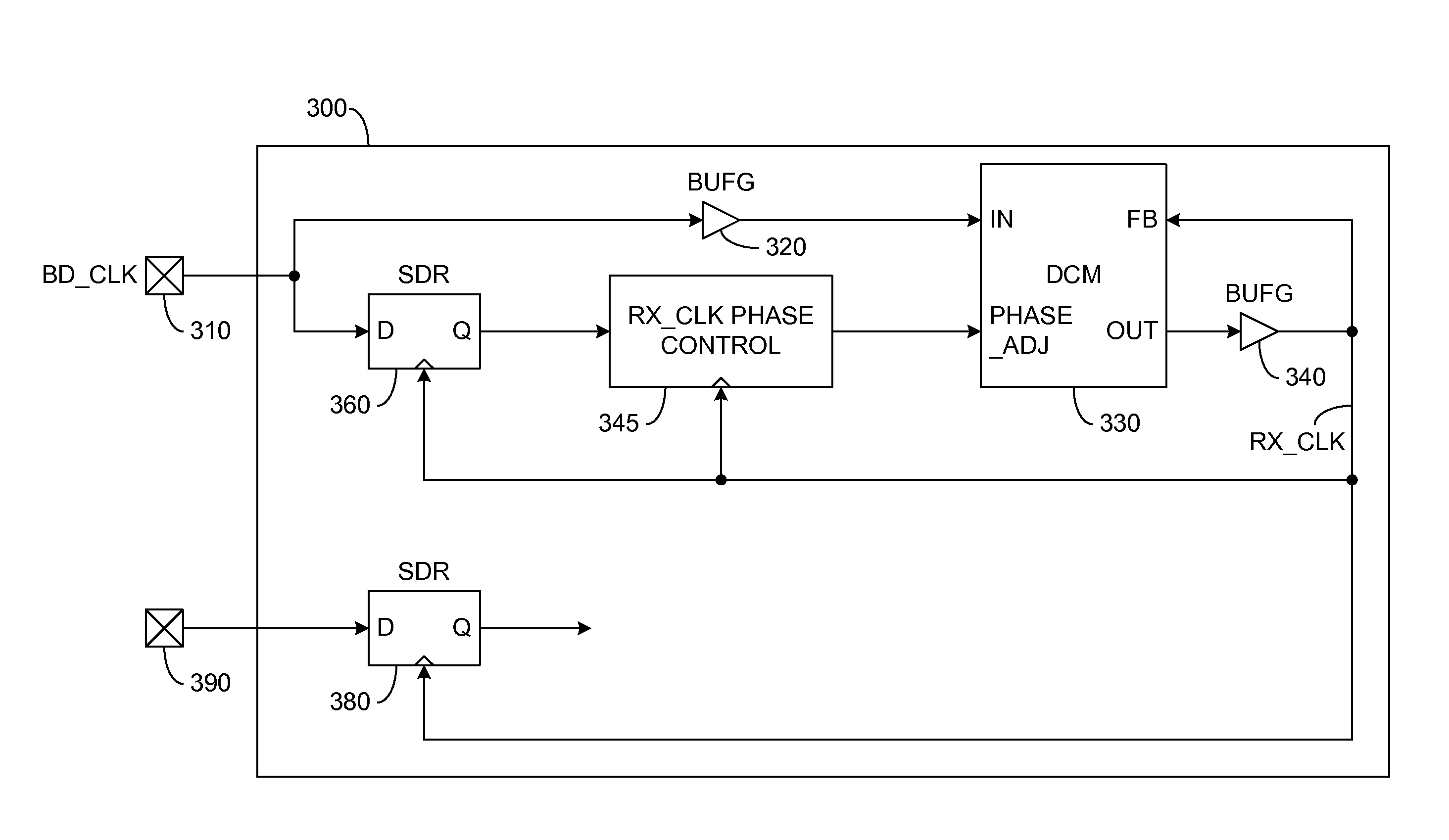
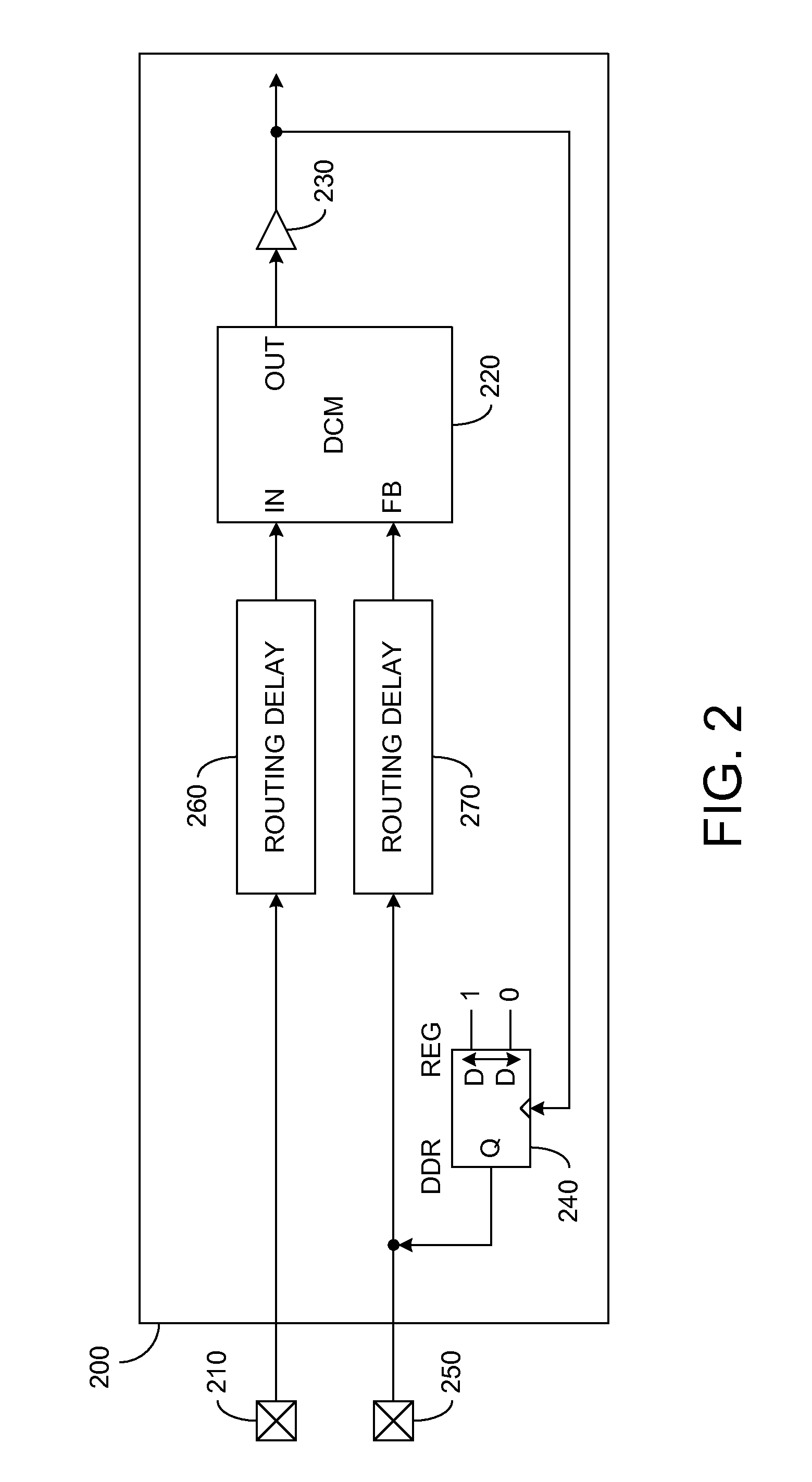
[0036]The Figures described above and the written description of specific structures and functions below are not presented to limit the scope of what Applicants have invented or the scope of the appended claims. Rather, the Figures and written description are provided to teach any person skilled in the art to make and use the inventions for which patent protection is sought. Those skilled in the art will appreciate that not all features of a commercial embodiment of the inventions are described or shown for the sake of clarity and understanding. Persons of skill in this art will also appreciate that the development of an actual commercial embodiment incorporating aspects of the present inventions will require numerous implementation-specific decisions to achieve the developer's ultimate goal for the commercial embodiment. Such implementation-specific decisions may include, and likely are not limited to, compliance with system-related, business-related, government-related and other c...


PUM


Abstract

Methods and apparatuses provide a clocked digital device having dynamically adjustable operating characteristics. The digital device comprises a digital clock management (“DCM”) circuit in which the amount of delay between receipt of an active edge of a clock signal at the input of the DCM circuit and appearance of an active edge of another clock signal at the output of the DCM circuit depends on a phase adjustment signal applied to the DCM circuit's phase adjust input. A phase adjustment circuit provides the phase adjustment signal to the DCM circuit's phase adjust input for controlling the amount of the delay between the clock signal at the input of the DCM circuit and the clock signal at the output of the DCM circuit.

Description

CROSS REFERENCE TO RELATED APPLICATIONS[0001]This application for patent is a continuation of U.S. Non-Provisional Application Ser. No. 12 / 624,267, entitled “Method And Apparatus For Clock Calibration In A Clocked Digital Device,” filed Nov. 23, 2009, which is incorporated herein by reference in its entirety.STATEMENT REGARDING FEDERALLY SPONSORED RESEARCH[0002]Not applicable.REFERENCE TO APPENDIX[0003]Not applicable.BACKGROUND OF THE INVENTION[0004]1. Field of the Invention[0005]This disclosure relates generally to methods and apparatuses for calibrating clocks in clocked digital devices.[0006]2. Description of the Related Art[0007]Many modern electronic devices operate based on clock signals that are provided to the device from an external source and / or generated internal to the electronic devices. Such devices are referred to herein as clocked digital devices.[0008]Because of their nature, clocked digital devices can and do exhibit a range of different performance characteristics...

Claims


Application Information

Patent Timeline
Patent Type & Authority Applications(United States)
IPC IPC(8): H03H11/26G06F1/04
CPCG06F1/10H03L7/0814H03K5/135
Inventor CAMP, CHARLES J.
Owner INT BUSINESS MASCH CORP
Why Eureka
Try Eureka