Nonvolatile memory device using interleaving technology and programmming method thereof

a non-volatile memory and programming technology, applied in static storage, digital storage, instruments, etc., can solve the problems of increased read-failure rate, increased threshold voltage, and reduced reliability, so as to reduce and/or minimize a number of total errors and increase reliability

Active Publication Date: 2011-09-08
SAMSUNG ELECTRONICS CO LTD
View PDF4 Cites 18 Cited by
  • Summary
  • Abstract
  • Description
  • Claims
  • Application Information

AI Technical Summary

Benefits of technology

[0011]One or more embodiments may provide a nonvolatile memory device using interleaving technology to reduce and / or minimize a number of total errors at the end of life (EOL), thereby increasing reliability at the EOL, and a programming method thereof.

Problems solved by technology

However, as the number of bits stored in a single memory cell increases, reliability may deteriorate and the read-failure rate may increase.
However, since the voltage window of a memory may be limited, the difference in a threshold voltage between adjacent bits may decrease as “m” increases, which may increase the read failure rate.
The difference in the number of read operations between pages may cause a bit error rate (BER) to be different from page to page.
However, it is difficult to adjust the verify-read voltage so that every page has the same BER at the EOL.
It is more difficult as the number of threshold voltage states increases.

Method used


Image

  • Nonvolatile memory device using interleaving technology and programmming method thereof
  • Nonvolatile memory device using interleaving technology and programmming method thereof
  • Nonvolatile memory device using interleaving technology and programmming method thereof

Examples


Embodiment Construction

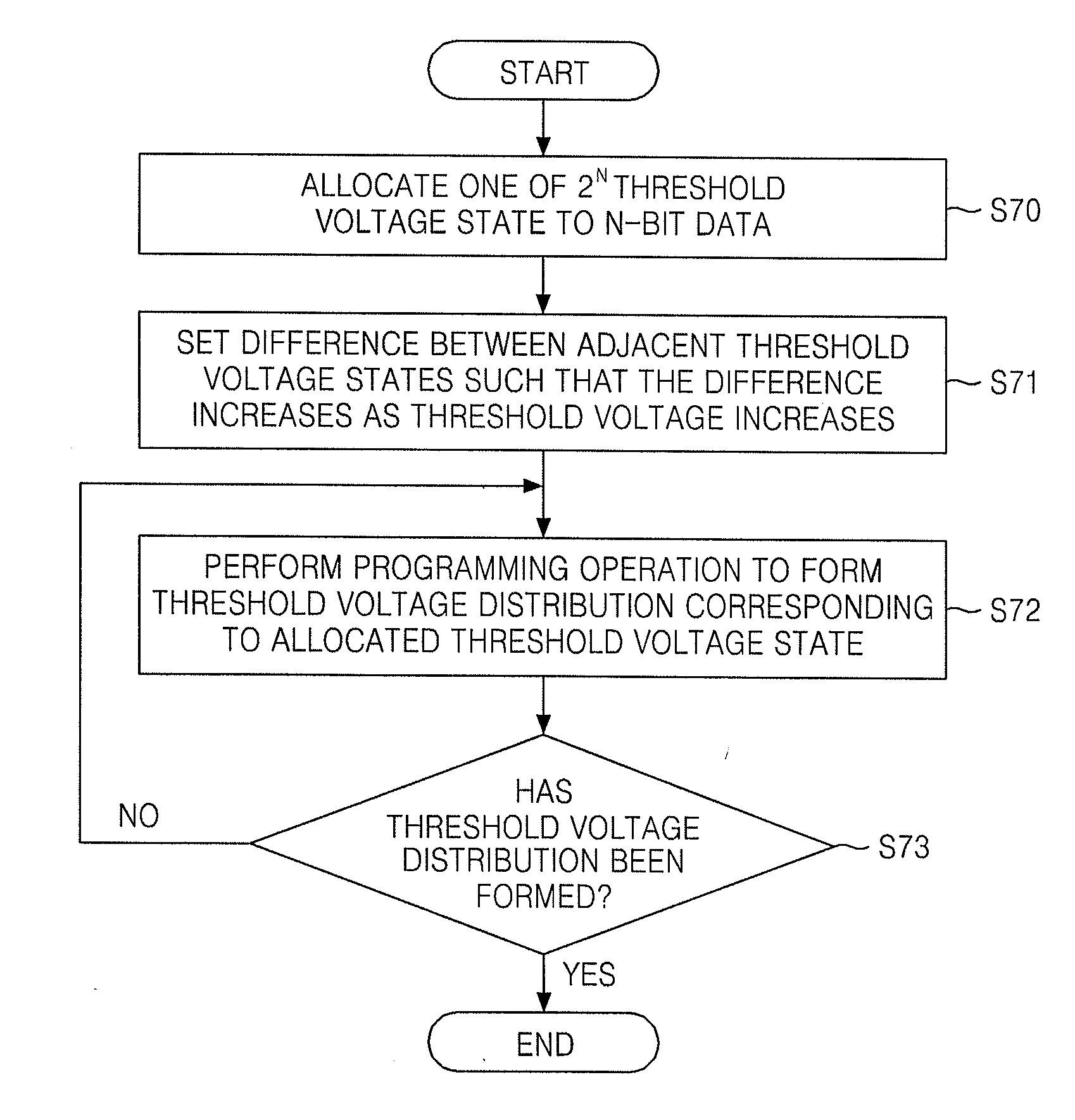
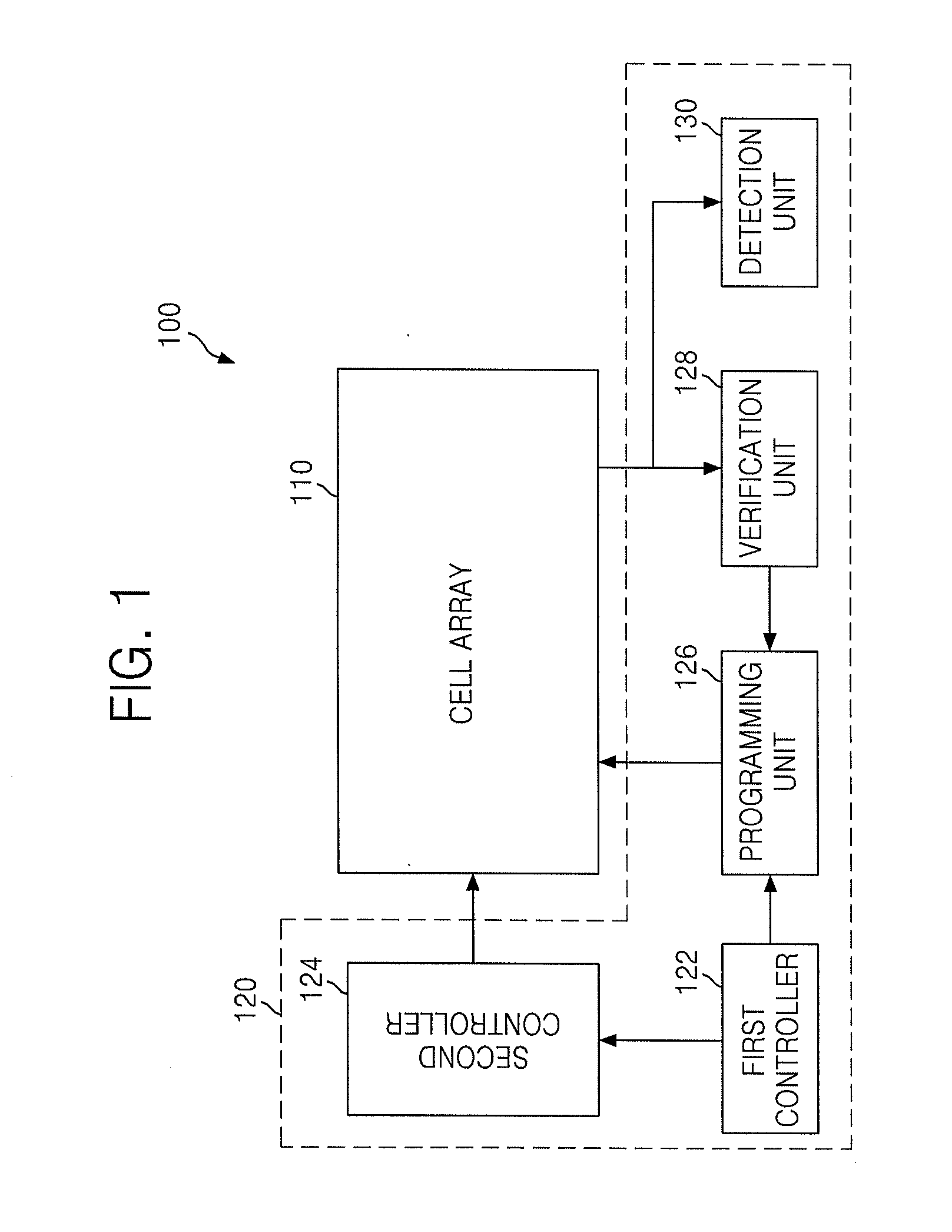
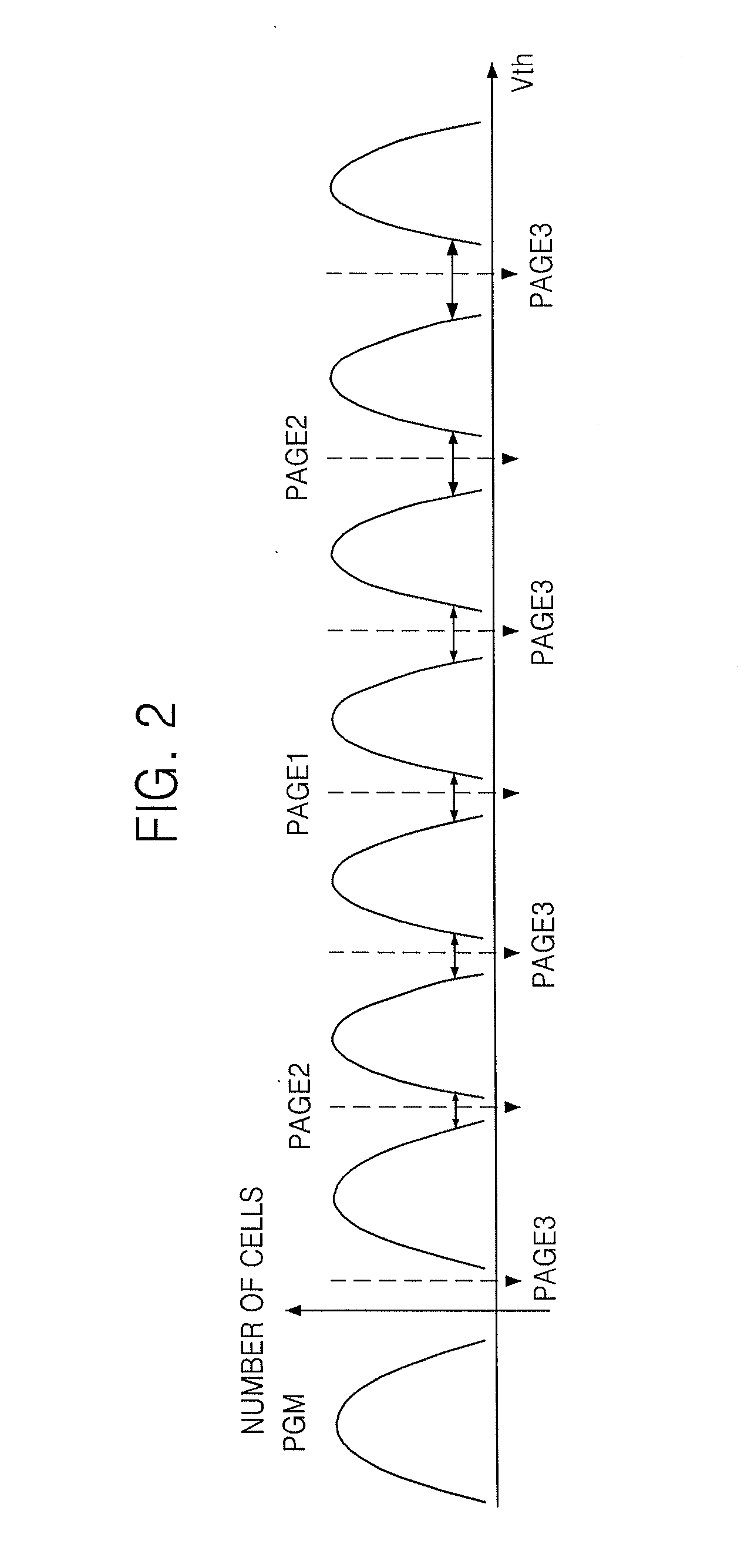
[0042]Exemplary embodiments will now be described more fully hereinafter with reference to the accompanying drawings; however, they may be embodied in different forms and should not be construed as limited to the embodiments set forth herein. Rather, these embodiments are provided so that this disclosure will be thorough and complete, and will fully convey the scope of the invention to those skilled in the art. Like reference numerals refer to like elements throughout the specification.

[0043]As used herein, the term “and / or” includes any and all combinations of one or more of the associated listed items and may be abbreviated as “ / ”. It will be understood that, although the terms first, second, etc. may be used herein to describe various elements, these elements should not be limited by these terms. These terms are only used to distinguish one element from another. For example, a first signal could be termed a second signal, and, similarly, a second signal could be termed a first si...


PUM


Abstract

A nonvolatile memory device using interleaving technology is provided. The nonvolatile memory device includes a first controller configured to allocate one of 2N threshold voltage states to N-bit data where N is 2 or a natural number greater than 2, a second controller configured to set a difference between adjacent threshold voltage states among the 2N threshold voltage states so that the difference increases as a threshold voltage increases, and a programming unit configured to form a threshold voltage distribution state corresponding to the allocated threshold voltage state and to program the N-bit data to a multi-level cell. The second controller controls the difference between the adjacent threshold voltage states to equalize the number of read errors for all intersections among the 2N threshold voltage states at the end of life.

Description

REFERENCE TO RELATED APPLICATIONS[0001]This application claims priority under 35 U.S.C. §119 to Korean Patent Application No. 10-2010-0020488, filed on Mar. 8, 2010, in the Korean Intellectual Property Office, and entitled: “Nonvolatile Memory Device Using Interleaving Technology and Programming Method Thereof,” which is incorporated by reference herein in its entirety.BACKGROUND[0002]1. Field[0003]Embodiments relate to a nonvolatile memory device, and more particularly, to a nonvolatile memory device using interleaving technology and a programming method thereof.[0004]2. Description of the Related Art[0005]Single-level cell (SLC) memory stores data of one bit in a single memory cell. SLC memory is also referred to as single-bit cell (SBC) memory. Data of one bit is written to and read from SLC memory by a voltage belonging to one of two distributions distinguished by a threshold voltage programmed to a memory cell.[0006]Programmed threshold voltages form a distribution in a predete...

Claims


Application Information

Patent Timeline
Patent Type & Authority Applications(United States)
IPC IPC(8): G11C16/10
CPCG11C16/10G11C11/5628G11C16/0483G11C16/12G11C16/30G11C16/34
Inventor EUN, HEE SEOKKIM, YONG JUNE
Owner SAMSUNG ELECTRONICS CO LTD
Why Eureka
Try Eureka