Test circuitry wafer

a test circuit and wafer technology, applied in the field of test circuitry wafers, can solve the problems of increasing the direct cost of manufacturing the probe card/needle, the long lead time needed to manufacture the probe needle, and the high cost of precision probe needle manufacturing, so as to reduce the precision requirement of the probe card, reduce or minimize the number of touchdowns on the device pad, and improve the efficiencies of both testing time and the manufacturing cost of the probe card

Inactive Publication Date: 2005-12-29
POLARIS INNOVATIONS
View PDF9 Cites 3 Cited by
  • Summary
  • Abstract
  • Description
  • Claims
  • Application Information

AI Technical Summary

Benefits of technology

[0013] Embodiments of the present invention generally provide apparatuses and methods for testing a device wafer having a plurality of devices formed thereon. One embodiment of the invention provides an interface wafer which serves as an interface between a device wafer having a plurality of devices formed thereon to be tested and a probe card of a testing system. In one embodiment, the interface wafer reduces the precision requirement of the probe cards utilized in testing systems for conducting wafer level tests. Additionally, in one embodiment, the interface wafer reduces or minimizes the number of touchdowns on device pads required to complete testing of the devices on the wafer. Furthermore, in one embodiment, the interface wafer improves efficiencies in both testing time and probe card manufacturing cost. Another embodiment of the invention provides an interface wafer which allows a single probe card design to be utilized for testing a variety of device designs.
[0014] Another embodiment provides a parallel test interface wafer and a method for performing parallel testing of devices formed on a device wafer. The parallel test interface wafer enables parallel testing of devices formed on a device wafer in a single touchdown which may achieve higher throughput in production testing. Particularly, the parallel test interface wafer may improves efficiency in conducting burn-in tests performed at the wafer level.
[0015] Yet another embodiment provides a test circuitry wafer which incorporates design-for-test features that are typically implemented on-chip and simplifies device designs by removing the design-for-test features from the device / chip. Removal of some or all DFT features from the devices on the wafer to the test circuitry wafer reduces the substrate areas and routing space allocated to accommodate the DFT features on the device wafer. Furthermore, the devices one the device wafer may be designed to allow stronger power rails, and signal routing between components within each device may be designed more efficiently because of the removal of the DFT features from the devices. Another advantage achieved by removing the DFT feature off-chip is that the performance impact to normal operation caused by the on-chip DFT blocks is minimized or substantially reduced because the DFT features are moved off-chip.

Problems solved by technology

As device feature sizes decrease with improved semiconductor processing techniques, the precision requirement for the probe needles becomes more stringent (e.g., smaller sizes and smaller tolerances), and the direct cost for manufacturing the probe cards / needles increases tremendously because of the strict precision requirement.
Associated with the high cost for manufacturing precision probe needles is a longer lead time needed to manufacture the probe needles.
Unless the orders for the probe card are placed far in advance, costly delays between production and testing of the device wafers are likely to occur, which may result in missed market opportunities and / or loss of first product status.
However, if an order was placed too far in advance, the probe card may be in production stages that cannot incorporate changes corresponding to additional changes (after the probe-card has been ordered) to the design of the devices to be formed on the wafer.
Furthermore, the probe card and probe needles manufactured for one specific device design on a wafer are generally incompatible (i.e., not reusable) for other device designs with different device sizes or leads.
Although the probe needles may be re-worked in some instances to allow some reusability, re-working the probe needles is a slow, tedious and relatively expensive task, and the re-worked probe needles provide lower quality and may become unreliable because of the re-work process.
Another problem encountered in conventional testing systems is that a testing system having one probe card cannot test all devices on a wafer all at once and requires sequential testing of groups of devices, resulting in prolonged testing time and reducing throughput.
Because all of the devices on the wafer cannot be tested at the same time (e.g., cannot be tested with the same touchdown), some tests may require excessively long time periods to complete, particularly with tests such as burn-in tests which may require days to complete for all devices on a wafer.
Such excessive time requirements for performing device testing substantially reduces production efficiencies and throughput.
Furthermore, a probe card may require an excessive number of touchdowns on the device pads on the wafer, which may result in damages to the devices formed on the wafer.
Another problem associated with testing of device wafers relates to the increasing design-for-test (DFT) features included on-chip for testing and manufacturing.
As more DFT features are included on-chip, the area or space required to implement the on-chip DFT features increases along with the additional design effort required to accommodate all components of the device in a limited substrate area.
Also, the performance of the device may be hindered due to the on-chip DFT features.
Thus, the additional effort required for implementing the DFT features on-chip have resulted in a reduction in the savings and utility of having the DFT features on-chip.
However, this is usually done as an after-thought because priority to optimize DFT features is low as compared to the need to optimize the main device performance.
This becomes especially critical in areas where congestions for routing normal operation signal already exist, resulting in increased layout time, weakened power rails and / or weakened device operation signal.
However, the performance impact to normal operation has also become difficult to control as the number of DFT features grows and complexity increases.
As sales of devices at the wafer level become more prevalent, the probe card cost has also become an increasingly important part of the test cost.

Method used


Image

  • Test circuitry wafer
  • Test circuitry wafer
  • Test circuitry wafer

Examples


Embodiment Construction

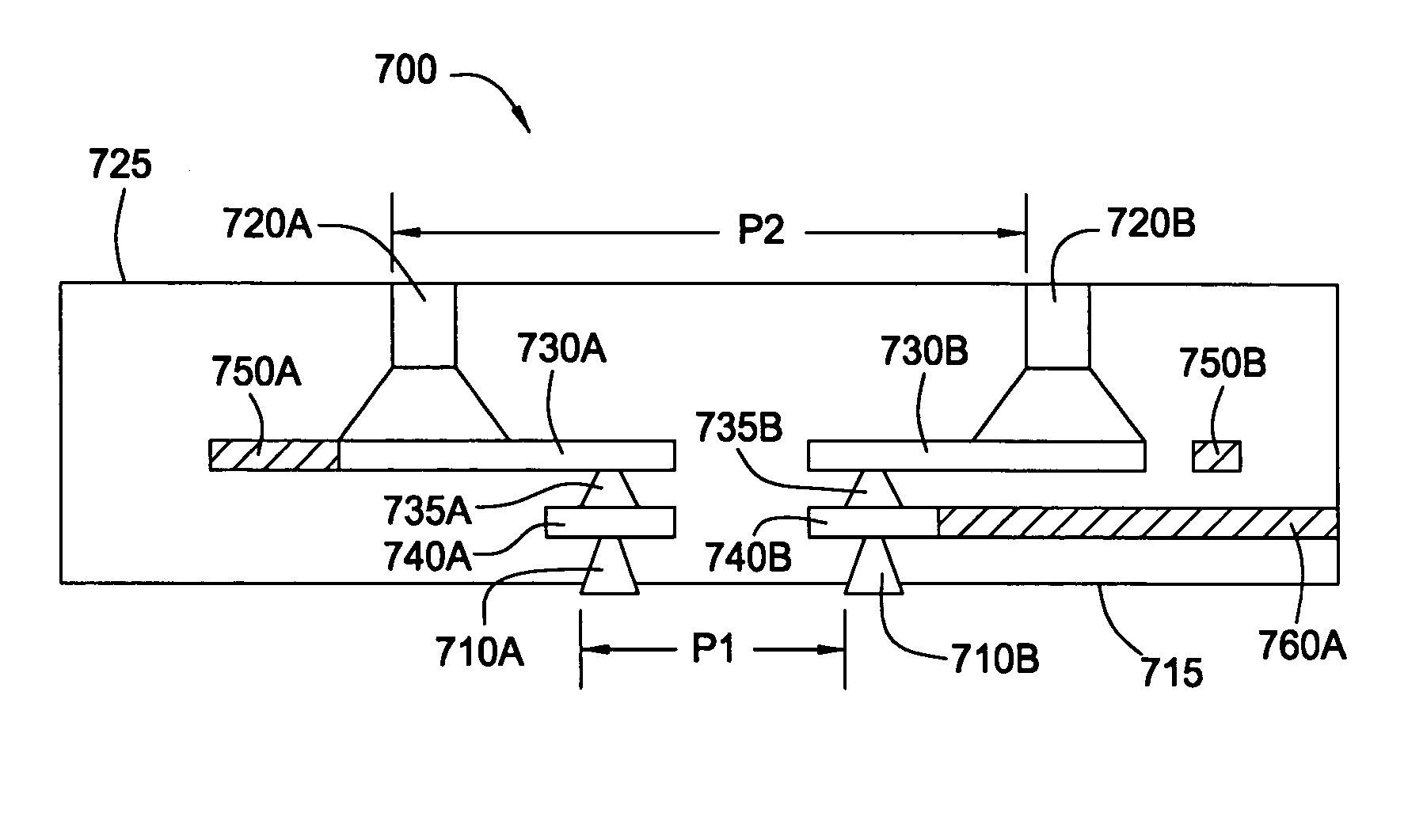
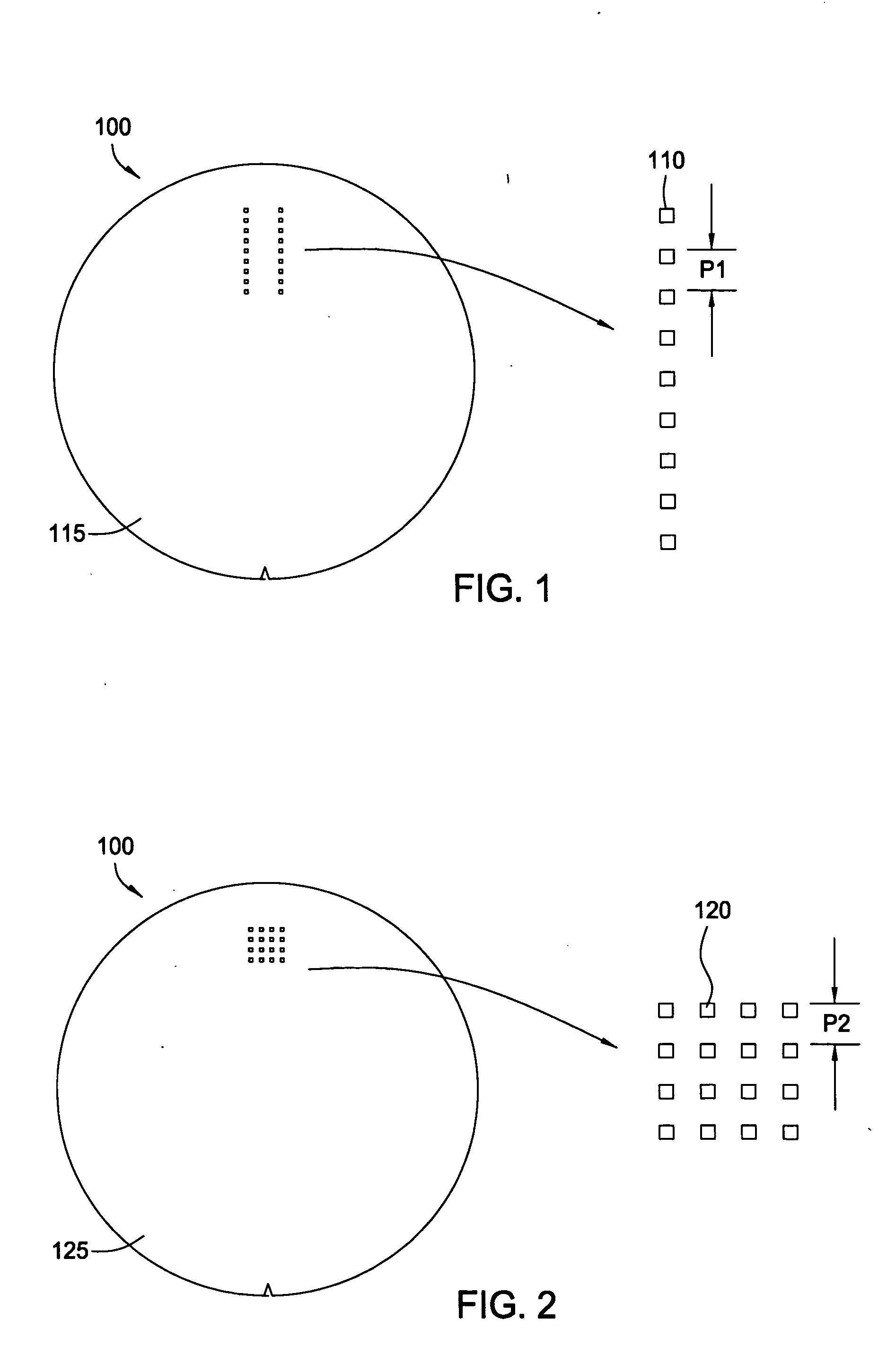
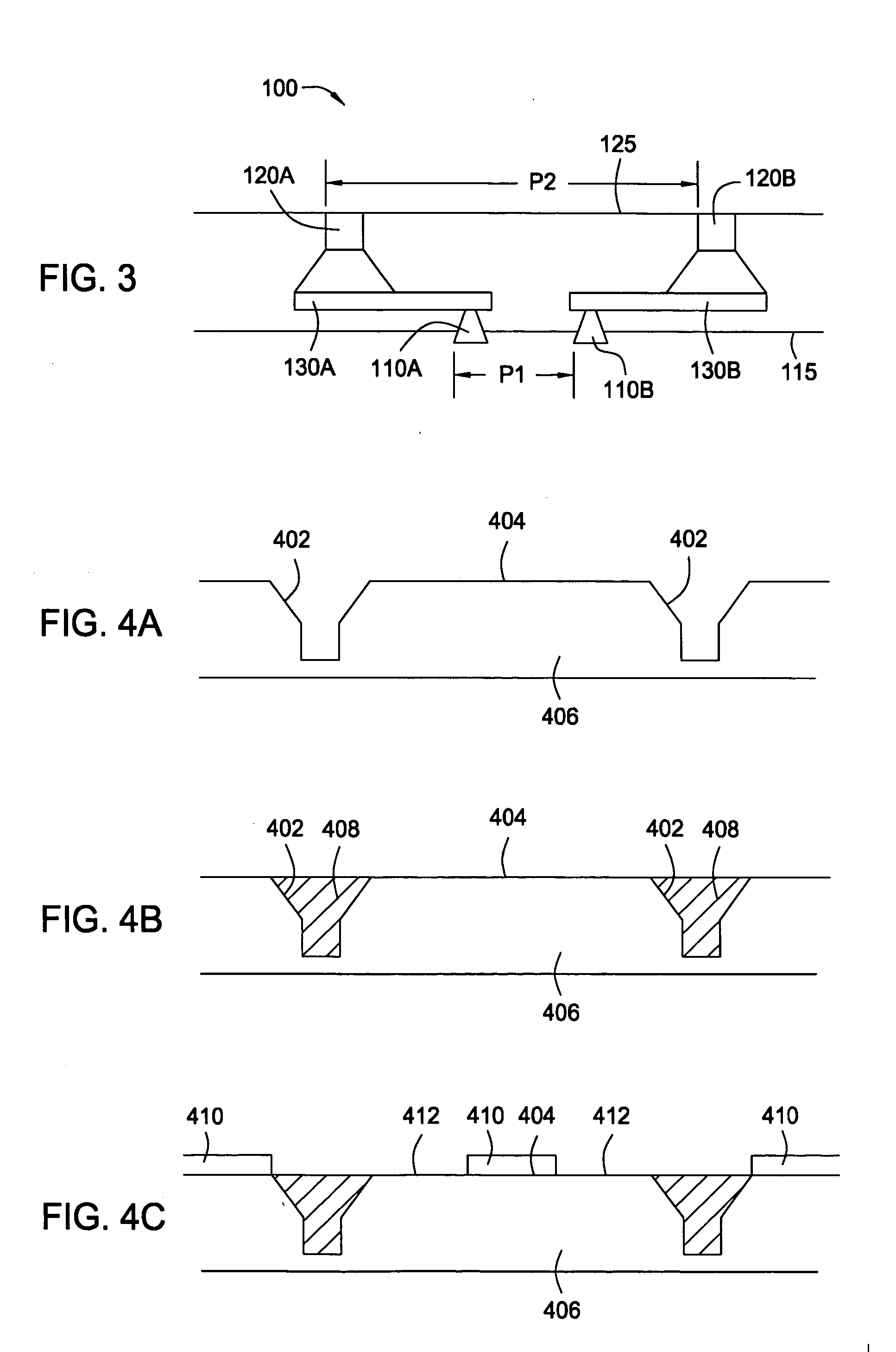
[0030] Embodiments of the present invention generally provide apparatuses and methods for testing a device wafer having a plurality of devices formed thereon. One embodiment provides an interface wafer which serves as an interface between a device wafer having a plurality of devices formed thereon to be tested and a probe card of a testing system. Another embodiment provides a parallel test interface wafer which facilitates parallel testing of devices formed on a device wafer. Yet another embodiment provides a test circuitry wafer which incorporates design-for-test features that are typically implemented on-chip and simplifies device designs by removing the design-for-test features from the device / chip.

[0031] In the following, reference is made to embodiments of the invention. However, it should be understood that the invention is not limited to specific described embodiments. Instead, any combination of the following features and elements, whether related to different embodiments ...


PUM


Abstract

Method and apparatus for testing a plurality of devices on a device wafer. One embodiment provides a test circuitry wafer having a first surface and a second surface, the test circuitry wafer comprising a plurality of contact pads disposed on the first surface for contacting a plurality of device pads on the device wafer, a plurality of interface pads disposed on the second surface for contacting probe needles on a probe card and one or more test features disposed in the test circuitry wafer, wherein the one or more test features are electrically connected to at least one of the contact pads and the interface pads.

Description

BACKGROUND OF THE INVENTION [0001] 1. Field of the Invention [0002] The present invention generally relates to an apparatus and method for testing a device wafer having a plurality of devices formed thereon, and more particularly, to an interface for connecting a probe card of a testing system to device pads on a device wafer. [0003] 2. Description of the Related Art [0004] In conventional semiconductor manufacturing, a plurality of integrated circuits or devices are formed on a semiconductor substrate or wafer, and after completing the fabrication processes, the devices formed on the wafer may be cut from the wafer and packaged into individual chips, which are then tested individually to ensure that each chip performs according to certain specification. To reduce costs associated with testing chips individually, the devices formed on the wafer may be tested prior to being separated into individual chips. Conducting tests on devices formed on a wafer improves cost efficiencies gener...

Claims


Application Information

Patent Timeline
Patent Type & Authority Applications(United States)
IPC IPC(8): G01R31/02G01R31/28
CPCG01R31/2889
Inventor MA, DAVID SUITWAI
Owner POLARIS INNOVATIONS
Why Eureka
Try Eureka