Plasma etching method and plasma etching apparatus

a plasma etching and plasma technology, applied in the direction of electrical equipment, decorative arts, electric discharge tubes, etc., can solve the problems of difficult to achieve uniform line width cd (critical dimension) and line height, and the inability to perform an etching process with high uniform line width of lines formed on the wafer, and achieve high uniformity in cross sectional shapes.

Inactive Publication Date: 2011-09-15
TOKYO ELECTRON LTD
View PDF5 Cites 23 Cited by
  • Summary
  • Abstract
  • Description
  • Claims
  • Application Information

AI Technical Summary

Benefits of technology

[0020]In accordance with the present disclosure, it is possible to independently control distributions of widths and heights of lines in a surface of a wafer and it is also possible to perform an etching process with high uniformity in cross sectional shapes of lines when the lines are formed by etching a layered mask film including an inorganic film and an organic film or when multiple kinds of line groups having various gaps between adjacent lines are formed by etching a mask film.

Problems solved by technology

However, recently, in manufacturing a semiconductor device, a wafer becomes larger.
As the wafer becomes larger, it becomes difficult to obtain uniformity in line widths CD (critical dimension) and a height of lines formed on the surface of the wafer.
However, in case of using the above-described plasma etching apparatuses to perform a plasma etching process, there are some problems as follows.
However, as described above, when a pattern having both a sparse area and a dense area is required, it is impossible to perform an etching process with high uniformity in line widths of the lines formed on a wafer.
Thus, it is difficult to control the etching rate to a required level by controlling the supply amount or composition ratio of the processing gas.
Consequently, line widths and heights of the lines in the surface of the wafer cannot be uniformed and cross sections of the lines cannot be uniformed.
In case of using the processing gas having the radicals of the low reaction rate, even if the temperature of the wafer and the supply amount or composition ratio of the processing gas are adjusted within a typical variable range, an amount of reacted radicals is hardly changed and the line widths of the lines cannot be controlled.

Method used


Image

  • Plasma etching method and plasma etching apparatus
  • Plasma etching method and plasma etching apparatus
  • Plasma etching method and plasma etching apparatus

Examples


first embodiment

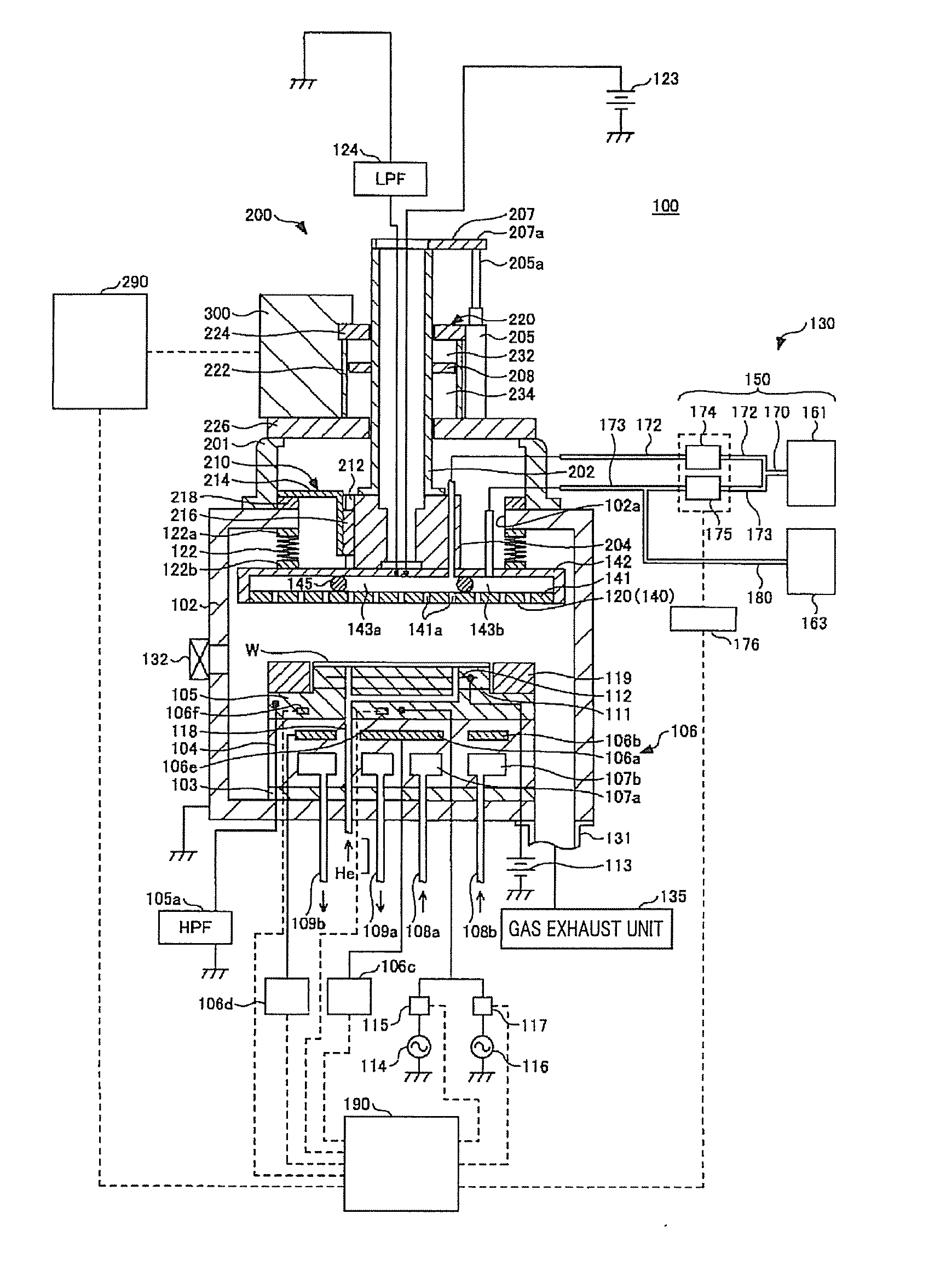
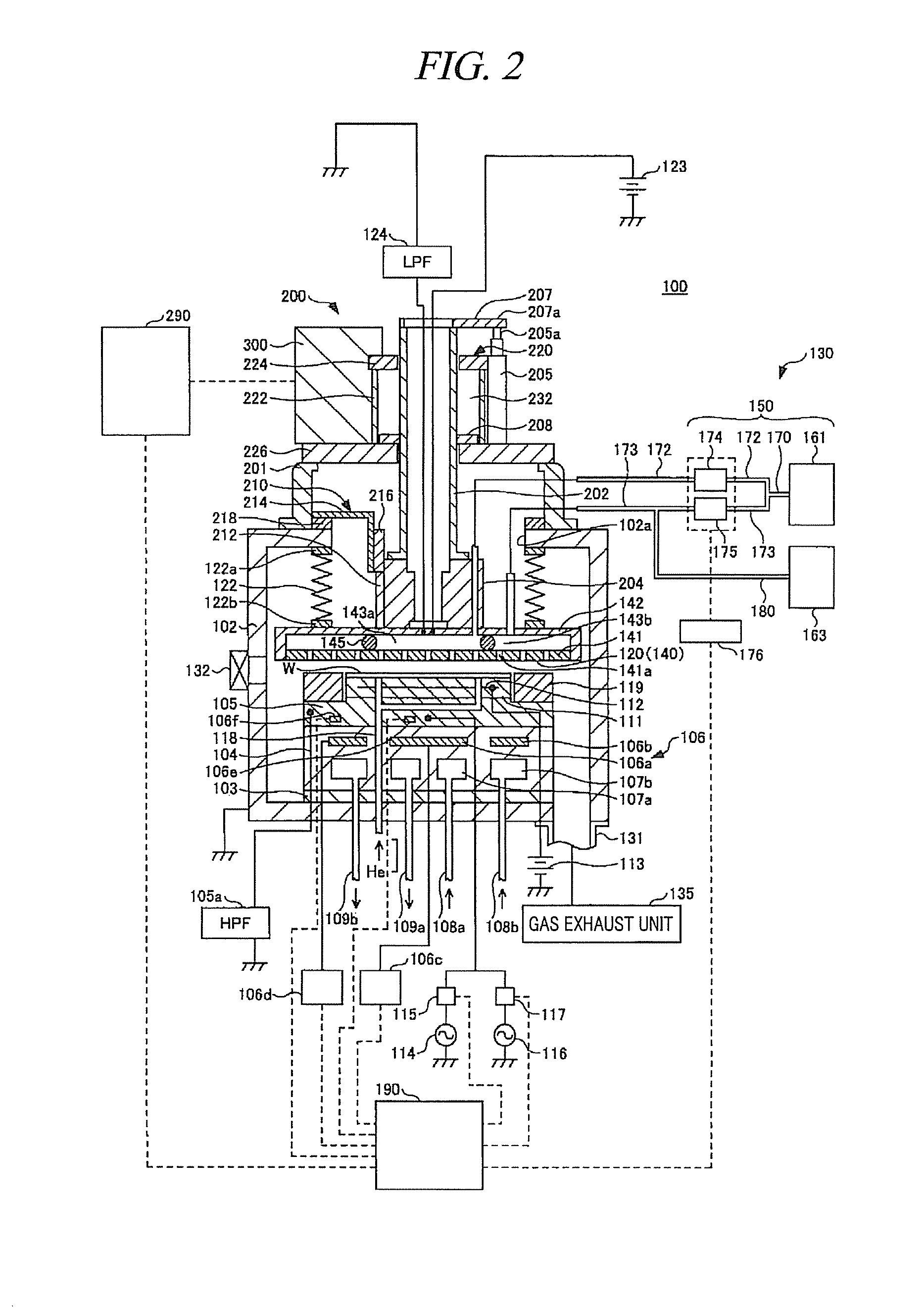
[0041]Referring to FIGS. 1 to 10D, a plasma etching method and a plasma etching apparatus in accordance with a first embodiment of the present disclosure will be explained.

[0042]First of all, referring to FIGS. 1 and 2, a plasma etching apparatus in accordance with the present embodiment will be explained. FIGS. 1 and 2 are cross sectional views showing schematic configurations of the plasma etching apparatus in accordance with the present embodiment. FIG. 1 shows a configuration in which an upper electrode is located at a retreat position, and FIG. 2 shows a configuration in which the upper electrode is located at a process position.

[0043]A plasma etching apparatus 100 in accordance with the present embodiment is configured as a parallel plate type plasma etching apparatus, for example.

[0044]The plasma etching apparatus 100 includes a cylindrical chamber (processing vessel) 102 made of, for example, aluminum of which surface is anodically oxidized (alumite treated). The chamber 102...

modification example of first embodiment

[0191]Hereinafter, a plasma etching method and a plasma etching apparatus in accordance with a modification example of the first embodiment will be explained.

[0192]The present modification example is different from the first embodiment in that when an organic film is etched, a processing gas having a high adhesion coefficient and having radicals of a high reaction rate is used in a second mask film etching process.

[0193]In the present modification example, the plasma etching apparatus explained with reference to FIGS. 1 to 5 may be used, as in the first embodiment. Further, as the first embodiment, a plasma etching method in accordance with the present modification example also includes a resist pattern forming process (step S11), an anti-reflective coating etching process (step S12), a second mask film etching process (step S13), a first mask film etching process (step S14), and an etching target film etching process (step S15) explained with reference to FIG. 6. Furthermore, a waf...

second embodiment

[0206]Hereinafter, referring to FIGS. 11 to 15, a plasma etching method and a plasma etching apparatus in accordance with a second embodiment of the present disclosure will be explained.

[0207]The present embodiment is different from the first embodiment in that a distribution of a gas supply amount in a wafer surface is not adjusted and a pattern to be formed does not have a sparse area but only has a dense area.

[0208]Referring to FIGS. 11 to 15, the plasma etching apparatus in accordance with the present embodiment will be elaborated. FIGS. 11 and 12 are cross sectional views showing a schematic configuration of the plasma etching apparatus in accordance with the present embodiment. To be specific, FIG. 11 shows a configuration in which an upper electrode is located at a retreat position, and FIG. 12 shows a configuration in which the upper electrode is located at a process position. FIGS. 13a and 13b provide explanatory diagrams simply showing an upper electrode driving unit. To b...


PUM

PropertyMeasurementUnit
DC voltageaaaaaaaaaa
frequencyaaaaaaaaaa
frequencyaaaaaaaaaa

Abstract

There are provided a plasma etching method and a plasma etching apparatus capable of independently controlling distributions of line widths and heights of lines in a surface of a wafer. The plasma etching method for performing a plasma etching on a substrate W by irradiating plasma containing charged particles and neutral particles to the substrate W includes controlling a distribution of reaction amounts between the substrate W and the neutral particles in a surface of the substrate W by adjusting a temperature distribution in the surface of the substrate W supported by a support 105, and controlling a distribution of irradiation amounts of the charged particles in the surface of the substrate W by adjusting a gap between the substrate W supported by the support 105 and an electrode 120 provided so as to face the support 105.

Description

CROSS-REFERENCE TO RELATED APPLICATION[0001]This application claims the benefit of Japanese Patent Application No. 2010-054828 filed on Mar. 11, 2010, the entire disclosures of which are incorporated herein by reference.FIELD OF THE INVENTION[0002]The present disclosure relates to a plasma etching method and a plasma etching apparatus for performing a plasma etching on a substrate.BACKGROUND OF THE INVENTION[0003]In manufacturing a semiconductor device, as an apparatus for processing a substrate such as a semiconductor wafer (hereinafter, referred to as “wafer”), there has been used a plasma etching apparatus which performs an etching process on the wafer by irradiating plasma to the wafer.[0004]By way of example, a wafer yet to be processed in the above-described plasma etching apparatus is formed of a silicon substrate. On the wafer, a silicon dioxide (SiO2) film, an etching target film formed of a polysilicon film, a mask film formed of a single layer or multiple layers, a bottom...

Claims


Application Information

Patent Timeline
Patent Type & Authority Applications(United States)
IPC IPC(8): C23F1/08C23F1/00
CPCH01J37/32091H01J37/32165H01J37/32568H01L21/31116H01L21/31122H01L21/3065H01L21/32139H01L21/67103H01L21/67109H01L21/6831H01L21/32137
Inventor YAEGASHI, HIDETAMIHONDA, MASANOBUSHIMIZU, AKITAKA
Owner TOKYO ELECTRON LTD
Why Eureka
Try Eureka