Dual vertical channel transistor and fabrication method thereof

a vertical channel transistor and vertical channel technology, applied in the field of dual-gate fin field effect transistors, can solve the problems of increasing the complexity of the front-end of line (feol) process, affecting the stability of the memory cell array threshold voltage (vsub>th/sub>), and the inability to meet the requirements of the threshold voltage. the effect of vsub>th/sub>

Active Publication Date: 2011-09-22
NAN YA TECH
View PDF2 Cites 30 Cited by
  • Summary
  • Abstract
  • Description
  • Claims
  • Application Information

AI Technical Summary

Benefits of technology

[0008]It is therefore the primary object of the invention to provide an improved dual vertical channel, dual-gate fin field-effect-transistor (FinFET) with buried bit line scheme to eliminate the above-mentioned prior art problems or shortcomings.

Problems solved by technology

However, front-end-of-line (FEOL) process becomes more complicated accordingly.
Gap fill with oxide film thus becomes an obstacle to dynamic random access memory (DRAM) shrinkage.
However, threshold voltage (Vth) stability for the memory cell array becomes much worse because of complicated fabricating process, including, for example, tedious embedded bit line formation steps, recess for spin-on-dielectric (SOD) formation steps, metal and n+ type poly defined transistor gate length.
Reducing Vth variation with longer channel length is also unfeasible under vertical dimension constraint.
Further, it has been known that the DRAM array incorporated with the aforesaid vertical FinFET structure with buried bit line scheme face different challenges.
For example, parasitic bipolar transistor induced by floating body effect, which causes array Vth instability during cell operation.

Method used


Image

  • Dual vertical channel transistor and fabrication method thereof
  • Dual vertical channel transistor and fabrication method thereof
  • Dual vertical channel transistor and fabrication method thereof

Examples


Embodiment Construction

[0014]In the following description, numerous specific details are given to provide a thorough understanding of the invention. However, it will be apparent to one skilled in the art that the invention may be practiced without these specific details. In order to avoid obscuring the present invention, some well-known configurations and process steps are not disclosed in detail.

[0015]Likewise, the drawings showing embodiments of the apparatus are semi-diagrammatic and not to scale and, particularly, some of the dimensions are for the clarity of presentation and are shown exaggerated in the FIGS. Also, where multiple embodiments are disclosed and described having some features in common, for clarity and ease of illustration and description thereof like or similar features one to another will ordinarily be described with like reference numerals.

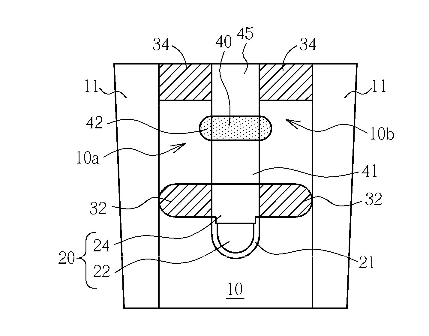
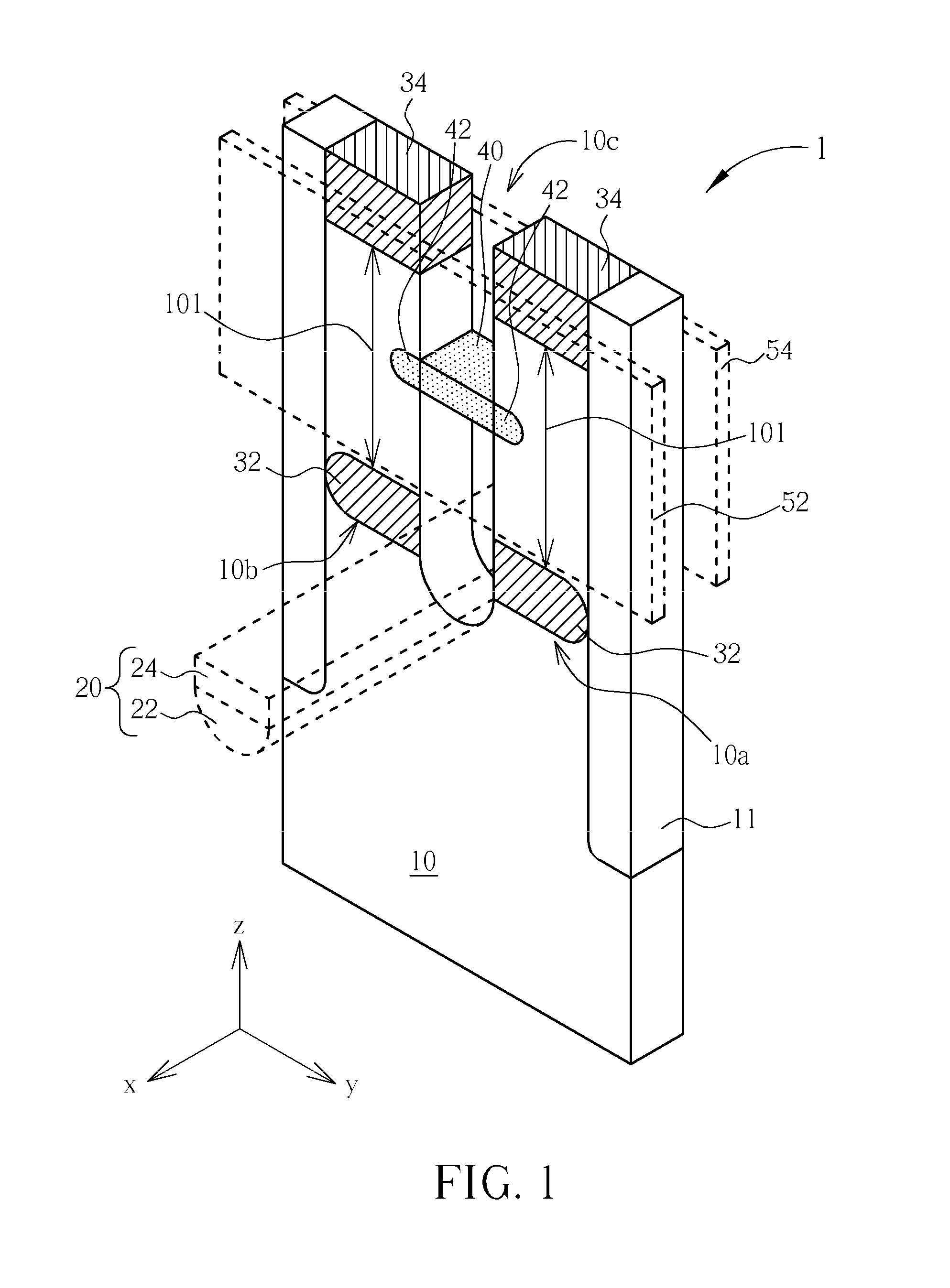
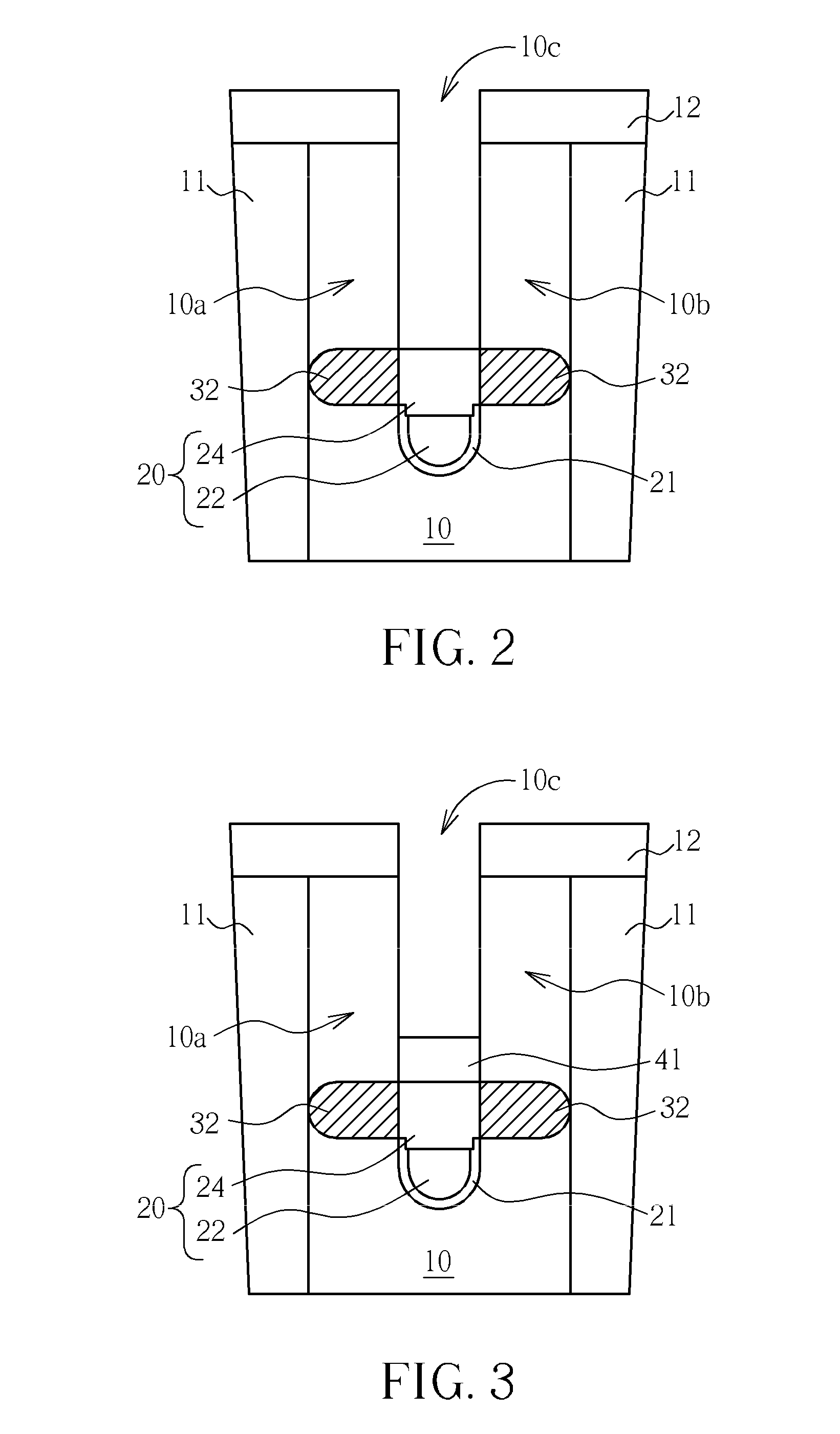
[0016]The preferred embodiment pertains to a dual vertical channel, dual-gate fin field-effect-transistor (FinFET) with buried bit line scheme hav...


PUM


Abstract

A dual vertical channel transistor includes a tuning fork-shaped substrate body; a buried bit line embedded at a bottom of a recess between two prong portions of the tuning fork-shaped substrate body; an out-diffused drain region adjacent to the buried bit line in the tuning fork-shaped substrate body; a source region situated at a top portion of each of the two prong portions of the tuning fork-shaped substrate body; an epitaxial portion connecting the two prong portions of the tuning fork-shaped substrate body between the out-diffused drain region and the source region; a front gate situated on a first side surface of the tuning fork-shaped substrate body; and a back gate situated on a second side surface opposite to the first side surface of the tuning fork-shaped substrate body.

Description

BACKGROUND OF THE INVENTION[0001]1. Field of the Invention[0002]The present invention relates generally to semiconductor devices. More particularly, this invention relates to a dual vertical channel, dual-gate fin field-effect-transistor (FinFET) with buried bit line scheme, and fabrication method thereof.[0003]2. Description of the Prior Art[0004]A vertical fin field-effect-transistor (FinFET) with embedded or buried bit line scheme has become the mainsteam for next-generation 4F2 (F stands for minimum lithographic feature width) cell because of simplified middle-of-line (MOL) process. However, front-end-of-line (FEOL) process becomes more complicated accordingly. For example, shallow trench isolation (STI) with half feature size and an aspect ratio of STI larger than 20 are required for 30 nm generation. Gap fill with oxide film thus becomes an obstacle to dynamic random access memory (DRAM) shrinkage.[0005]Vertical surrounding gate transistors (SGT) with embedded bit lines have b...

Claims


Application Information

Patent Timeline
Patent Type & Authority Applications(United States)
IPC IPC(8): H01L29/78
CPCH01L27/10823H01L27/10826H01L27/10876H01L27/10879H01L29/78642H01L29/1033H01L29/456H01L29/66666H01L29/7827H01L29/0657H10B12/36H10B12/34H10B12/056H10B12/053
Inventor RENN, SHING-HWA
Owner NAN YA TECH
Why Eureka
Try Eureka