
Data rate buffering in display port links

a data rate and buffering technology, applied in the field of display technology links, can solve problems such as interfering with video transmission

Active Publication Date: 2011-10-13
SYNAPTICS INC
View PDF3 Cites 17 Cited by
  • Summary
  • Abstract
  • Description
  • Claims
  • Application Information

AI Technical Summary

Benefits of technology

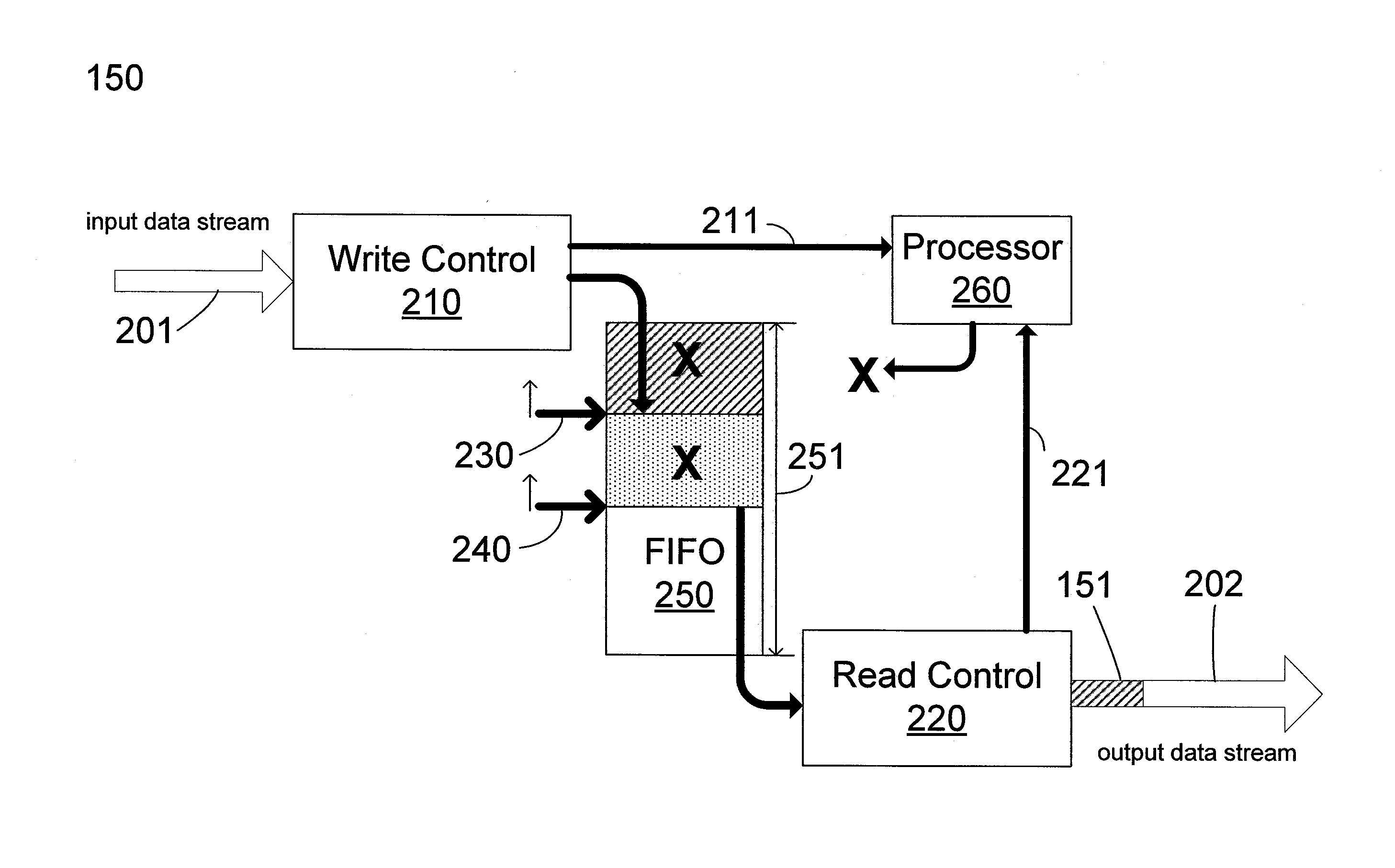
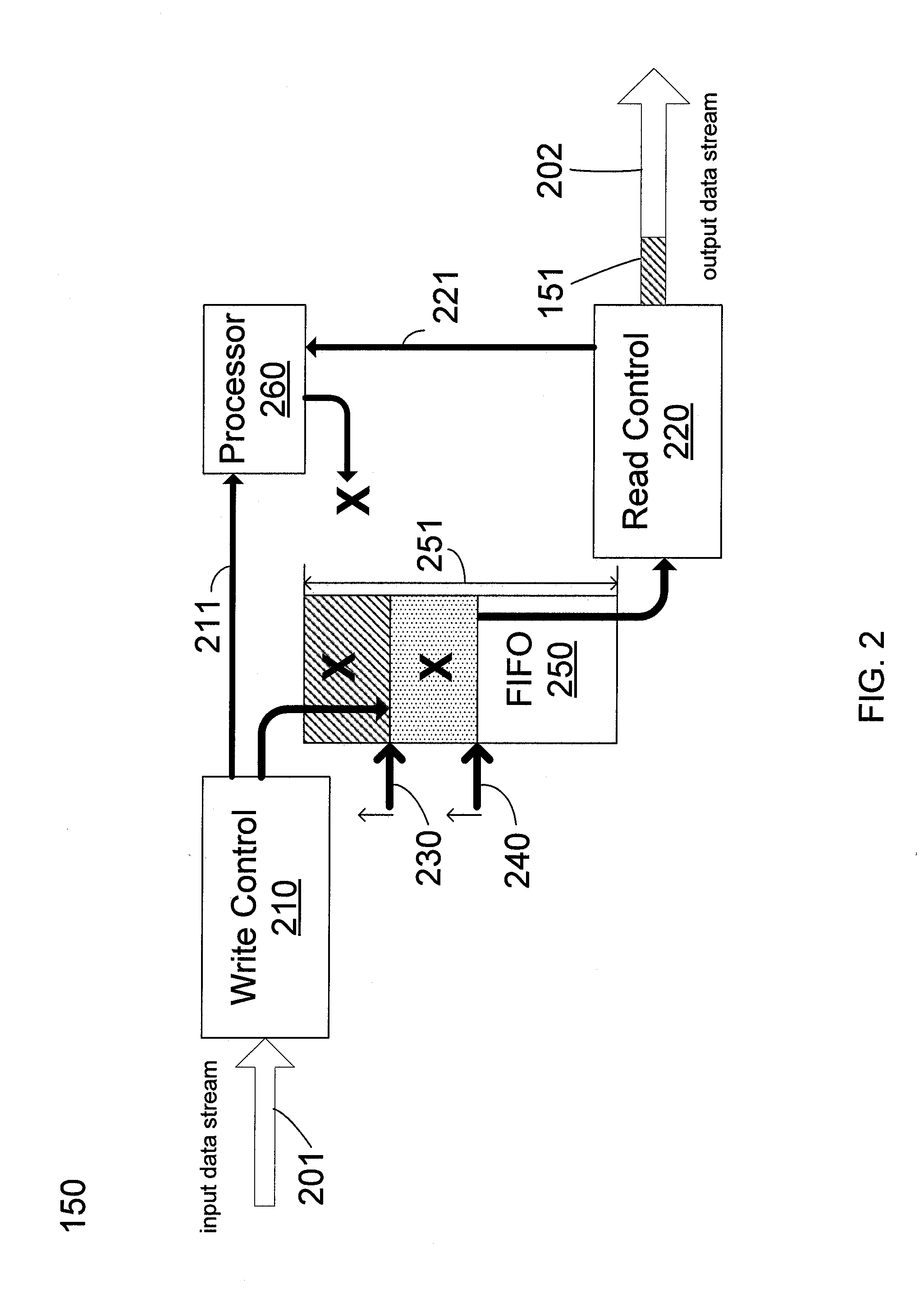
[0007]A rate matching device and a method for use in data links between a source device and a sink device is provided, including a first-in-first-out (FIFO) buffer having a write pointer, a read pointer, and a selected depth; a write control having a write clock to write an input data stream from the source device onto the FIFO buffer using the write pointer; a read control having a read clock to read data from the FIFO buffer using a read pointer, insert data to an output data stream and transmitting the data stream to the sink device; a processor to provide a bit number based on the write clock period and the read clock period further wherein the read control inserts data into the output data stream while the read pointer is stopped in the FIFO buffer to allow the write pointer to move ahead by the bit number provided by the processor, thereby avoiding a buffer overflow and a buffer underflow in the sink device.

Problems solved by technology

The issue of data rate matching arises for a data link between a source of imaging data (the Source device) and a receiver of the data (the Sink device).
By having such a mismatch in data rates between the source device and the sink device, underflow and overflow errors in the sink device buffer may be encountered, which may stall and break the data link, interrupting the video transmission.

Method used


Image

  • Data rate buffering in display port links
  • Data rate buffering in display port links
  • Data rate buffering in display port links

Examples


Embodiment Construction

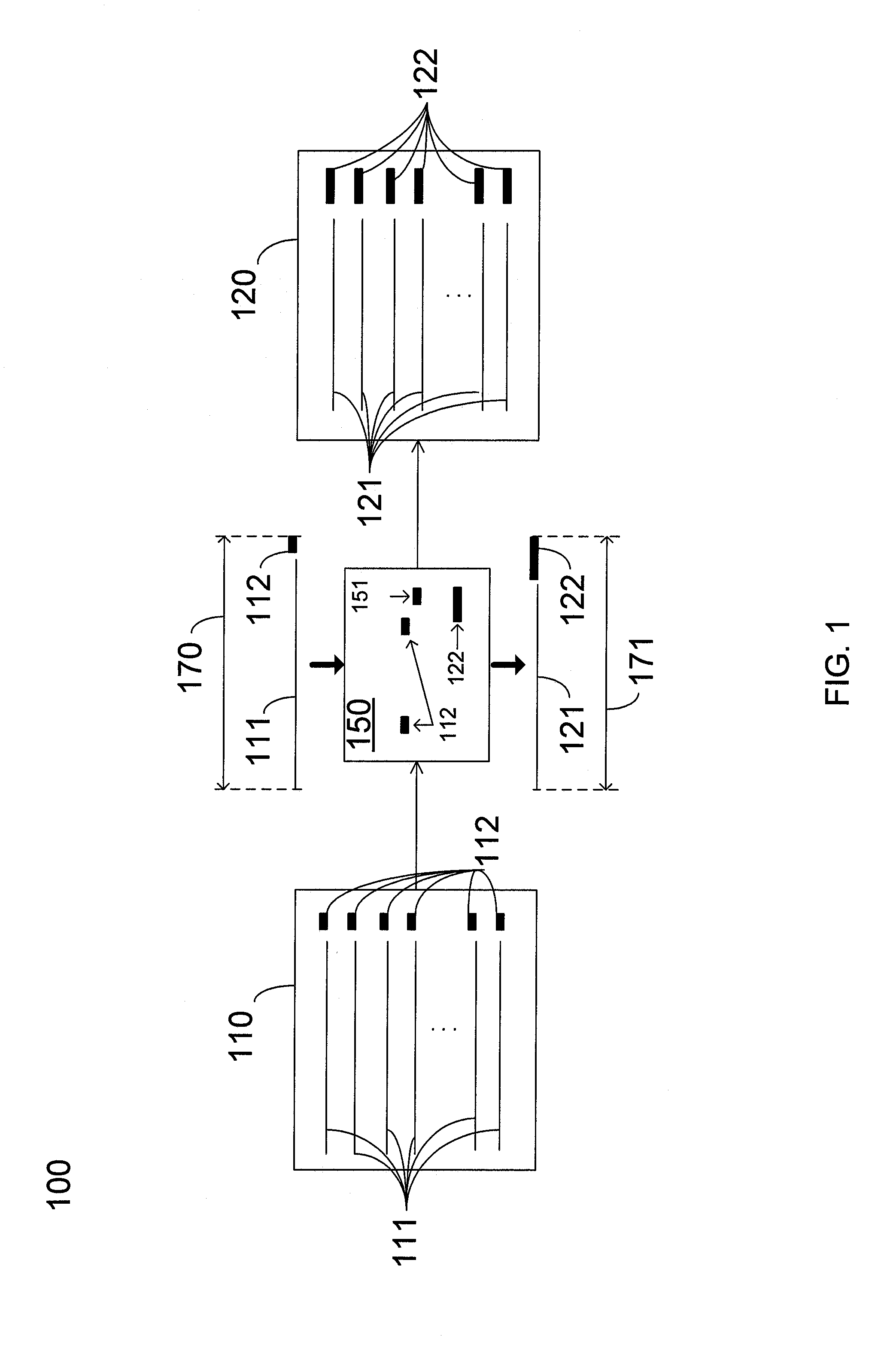
[0016]FIG. 1 illustrates a data link between a source device 110 and a sink device 120 according to some embodiments of the present invention. As shown in FIG. 1, a data transmission link 100 includes a source device 110, a sink device 120, and a rate matching device 150 coupled between source device 110 and sink device 120.

[0017]In embodiments that utilize a DisplayPort link, as described in the DP specification, a main link is provided between a transmitting display port (Tx) of source device 110, and a receiving display port (Rx) of sink device 120. The main link may include one, two, or four ac-coupled, doubly terminated differential pairs called lanes. The transmission lanes provide data transmission channels for the main link.

[0018]Some DP sources may not drive the data at a rate that is considered nominal by the DP specification. For example, the DP specs allow for the transmit (Tx) data rate to be between −5300 parts-per-million (ppm) and +300 ppm of the nominal data rate. T...


PUM


Abstract

Rate matching for use in data links between a source device and a sink device is provided. A rate matching device includes a first-in-first-out (FIFO) buffer having a write pointer and a read pointer; a write control having a write clock to write an input data stream from the source device onto the FIFO buffer using the write pointer; a read control having a read clock to read data from the FIFO buffer using a read pointer, insert data to an output data stream and transmitting the data stream to the sink device; a processor to provide a bit number based on the write clock period and the read clock period, wherein the read control inserts blanking data into the output data stream while the read pointer is stopped in the FIFO buffer to allow the write pointer to move ahead by the bit number provided by the processor. Some embodiments are thus able to avoid buffer overflow or underflow scenarios.

Description

BACKGROUND[0001]1. Field of the Invention[0002]The present invention relates to rate matching in display technology links and, in particular, to data rate buffering in data links.[0003]2. Discussion of Related Art[0004]Digital display technology for video streams is being widely adopted within the personal computer (PC) and consumer electronics (CE) industries. The VESA DisplayPort Standard, Version 1, Revision 1a of Jan. 11, 2008 for video data links (hereinafter DisplayPort, or DP), incorporated herein by reference in its entirety, is an example of a standard that may be used for transmission of video streams.[0005]The issue of data rate matching arises for a data link between a source of imaging data (the Source device) and a receiver of the data (the Sink device). In some cases, the source device transmits data at rates that differ from the display rate of the sink device. For example, different data rates may occur where a source intended for a protocol different from the DP st...

Claims


Application Information

Patent Timeline
Patent Type & Authority Applications(United States)
IPC IPC(8): H04N5/44H04N7/12
CPCH04N7/0105G09G5/001G09G5/006G09G5/12G09G2330/06G09G2350/00G09G2370/10G09G5/005G09G5/393
Inventor SHAMARAO, PRASHANT
Owner SYNAPTICS INC
Learn More