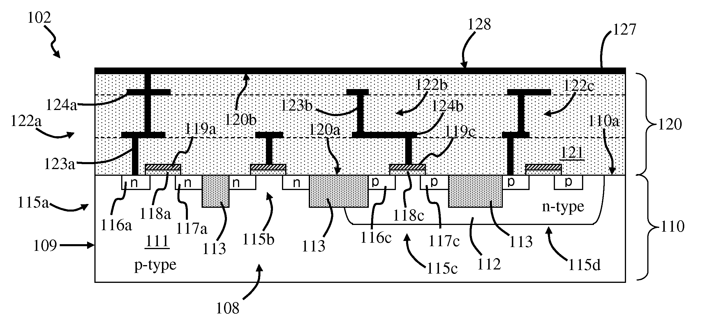
Semiconductor circuit structure and method of forming the same using a capping layer
a semiconductor and circuit structure technology, applied in semiconductor devices, semiconductor/solid-state device details, electrical apparatus, etc., can solve the problems of debris that can uncontrollably adjust the material quality debris can uncontrollably adjust the electrical and/or optical properties of layers subsequently formed, and the first portion of the semiconductor structure can flow undesiredly,
- Summary
- Abstract
- Description
- Claims
- Application Information
AI Technical Summary
Problems solved by technology
Method used
Image

Examples
Embodiment Construction
[0025]Information regarding how to make and use some of the embodiments of this disclosure can be found in several U.S. patents and patent applications by the same inventor as this disclosure. For example, information can be found in U.S. patent application Ser. Nos.:
[0026]11 / 092,498, filed on Mar. 29, 2005,
[0027]11 / 092,499, filed on Mar. 29, 2005,
[0028]11 / 092,500, filed on Mar. 29, 2005,
[0029]11 / 092,501, filed on Mar. 29, 2005;
[0030]11 / 092,521, filed on Mar. 29, 2005;
[0031]11 / 180,286, filed on Jul. 12, 2005;
[0032]11 / 378,059, filed on Mar. 17, 2006;
[0033]11 / 606,523, filed on Nov. 30, 2006,
[0034]11 / 873,719, filed on Oct. 17, 2007; and
[0035]11 / 873,769, filed on Oct. 17, 2007;
[0036]11 / 873,851, filed on Oct. 17, 2007,
the contents of all of which are incorporated by reference as though fully set forth herein.
[0037]Information regarding how to make and use some of the embodiments of this disclosure can be found in U.S. Pat. Nos. 7,052,941, 7,378,702, 7,470,142, 7,470,598, 7,632,738, 7,633...
PUM
 Abstract
Description
Claims
Application Information
 - Generate Ideas
- Intellectual Property
- Life Sciences
- Materials
- Tech Scout
- Unparalleled Data Quality
- Higher Quality Content
- 60% Fewer Hallucinations
Browse by: Latest US Patents, China's latest patents, Technical Efficacy Thesaurus, Application Domain, Technology Topic, Popular Technical Reports.
© 2025 PatSnap. All rights reserved.Legal|Privacy policy|Modern Slavery Act Transparency Statement|Sitemap|About US| Contact US: help@patsnap.com