

Method for fabricating semiconductor device and plasma doping apparatus
a technology of plasma doping apparatus and semiconductor device, which is applied in the direction of coating, chemical vapor deposition coating, electric discharge tube, etc., can solve the problem of difficult formation of low-resistance impurity region in the side portions of fin-type silicon region
- Summary
- Abstract
- Description
- Claims
- Application Information
AI Technical Summary
Benefits of technology
Problems solved by technology
Method used
Image

Examples
embodiment
[0064]A semiconductor device fabricating method of an embodiment and a plasma doping apparatus used in the fabricating method will be together described below with reference to the drawings.
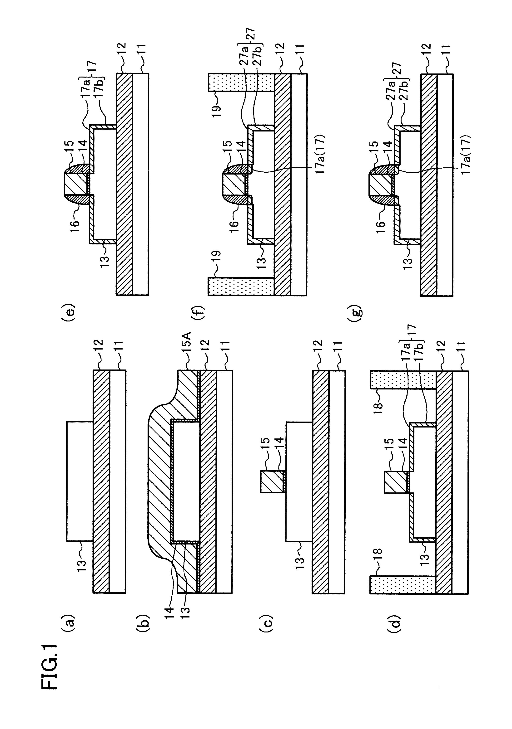
[0065]FIGS. 1(a)-1(g) are cross-sectional views illustrating steps in the semiconductor device fabricating method of the present embodiment.
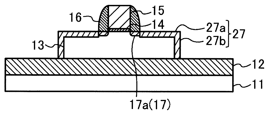
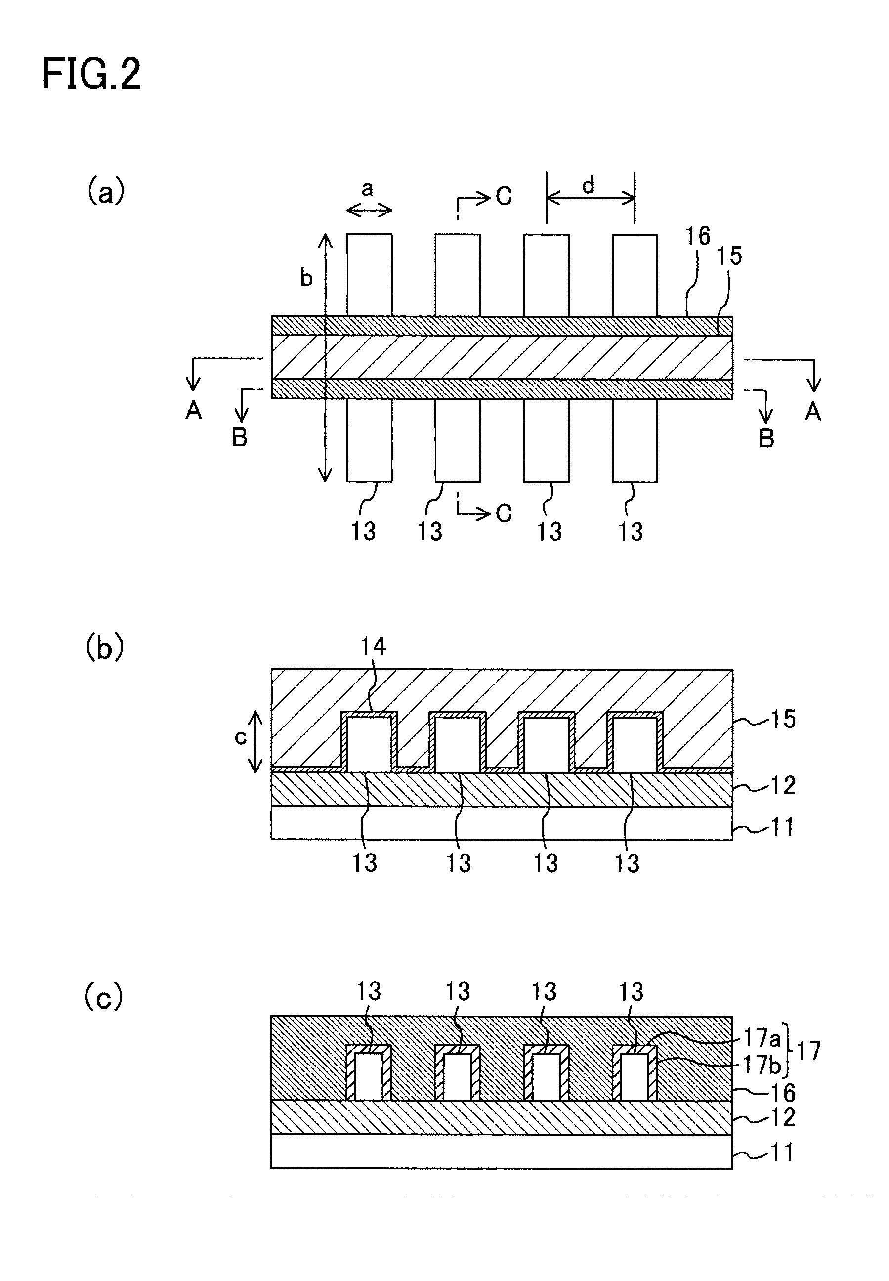
[0066]First, as illustrated in FIG. 1(a), a semiconductor-on-insulator (SOI) substrate is prepared, in which an insulating layer 12 made of, e.g., silicon oxide and having a thickness of 150 nm is provided on a support substrate 11 made of, e.g., silicon and having a thickness of 800 μm, and a semiconductor layer made of, e.g., silicon and having a thickness of 50 nm is provided on the insulating layer 12. Subsequently, the semiconductor layer is patterned, thereby forming a p-type fin-semiconductor region 13 which will be an active region. A width (a) of the fin-semiconductor region 13 in a gate width direction is, e.g., equal to or greater than 5 nm and equ...
PUM
| Property | Measurement | Unit |
|---|---|---|
| diameter | aaaaa | aaaaa |
| thickness | aaaaa | aaaaa |
| thickness | aaaaa | aaaaa |
Abstract
Description
Claims
Application Information