Touch panel
- Summary
- Abstract
- Description
- Claims
- Application Information
AI Technical Summary
Benefits of technology
Problems solved by technology
Method used
Image

Examples
first embodiment
[0046]FIG. 11 is a diagram illustrating the touch panel according to the present invention.
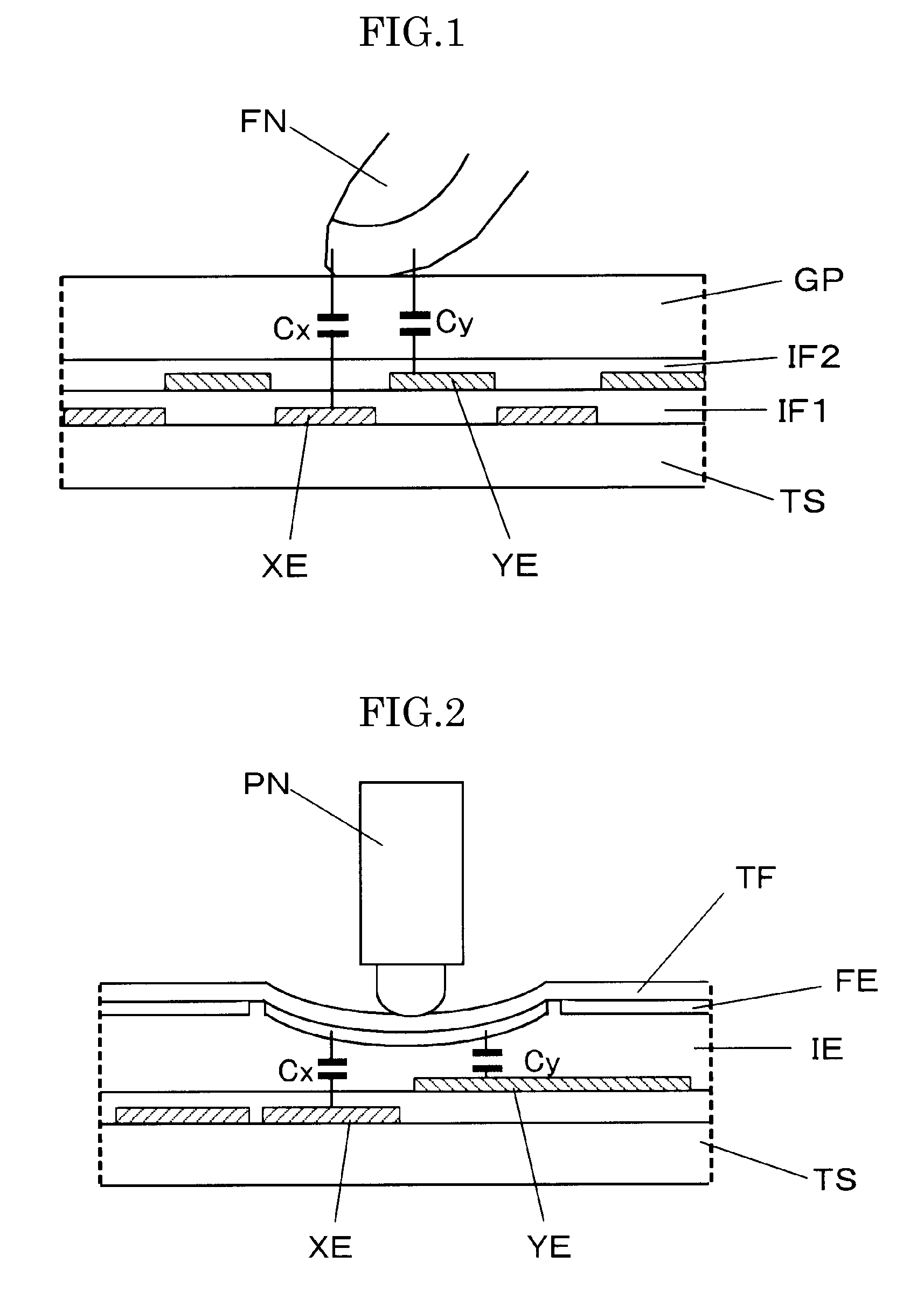
[0047]The touch panel according to the present invention is a touch panel of a capacitive coupling type, having; a first substrate (XYES) on which a coordinate detecting electrode for detecting XY coordinates of a point is formed; and a second substrate (UP) provided so as to face the above described first substrate, and is characterized in that the above described second substrate (UP) is provided with an elastic layer (EL) having a rigidity lower than the above described second substrate and a conductive layer (CL), the above described elastic layer (EL) and the above described conductive layer (CL) are layered in this order towards the above described first substrate (XYES), a non-conductive spacer (SP) is provided between the coordinated detecting electrode and the conductive layer, and a space created by the spacer is filled in with a liquid (LQ).
[0048]In the touch panel in FIG. 11, the c...
second embodiment
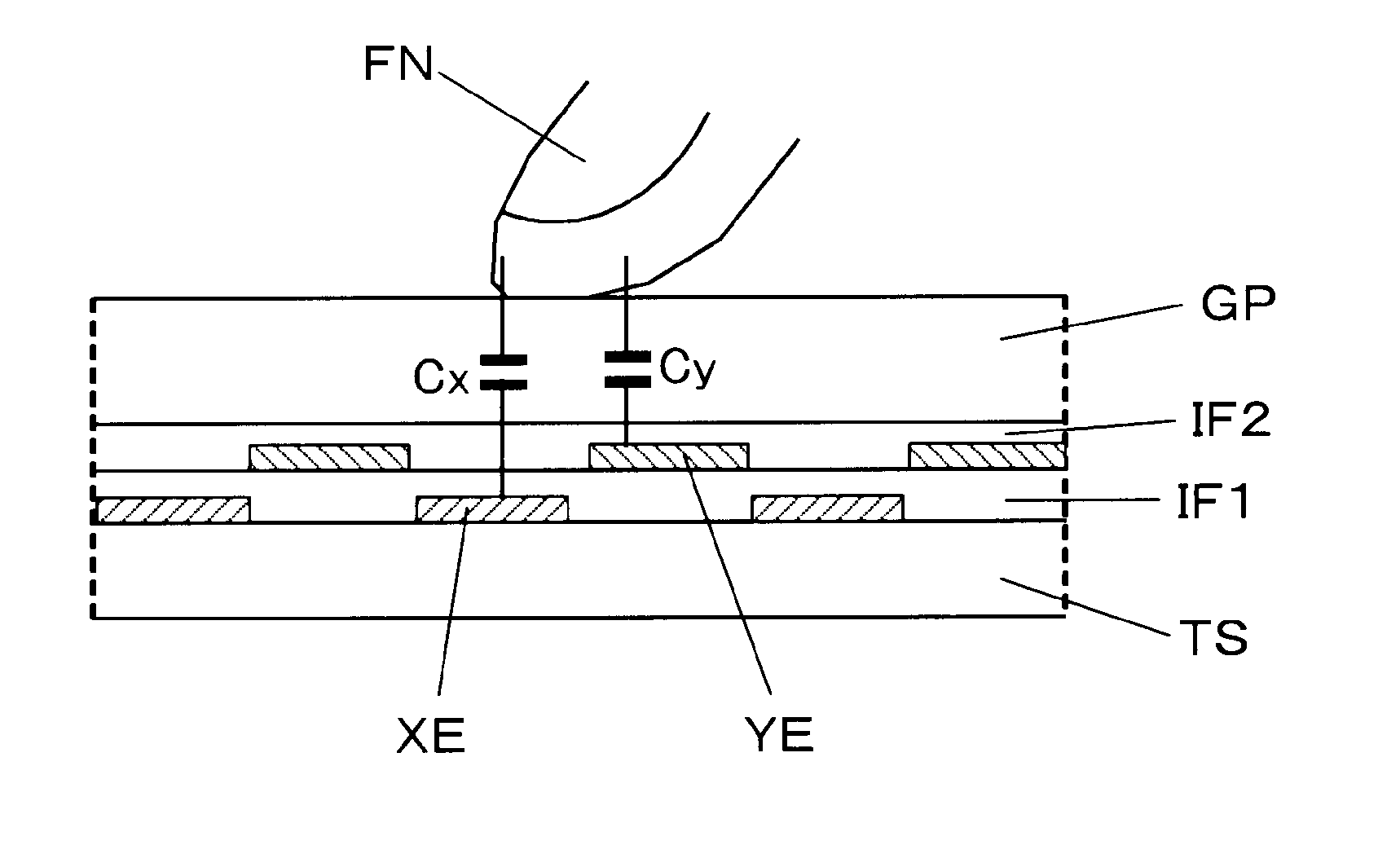
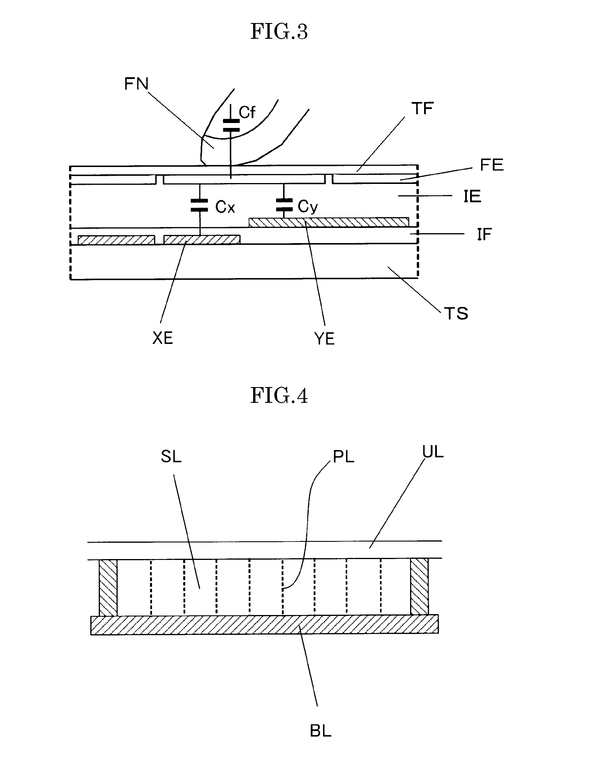
[0063]FIG. 14 is a diagram showing the structure of the touch panel according to the present invention, and is a cross sectional diagram showing the touch panel along line A-B in FIG. 13, which shows the arrangement of the electrodes. This cross sectional diagram shows only the layers that are necessary for describing the operation of the touch panel. In the figure, SUB and UP are transparent substrates, IF1 and IF2 are transparent insulating films, SP1 is spacers, which are beads, EL is a transparent elastic layer, and XP, YP and CL (conductive film) are electrodes for detection.
[0064]The touch panel according to the present embodiment is formed such that a transparent conductive film XP, a transparent first insulating film IF1, a transparent conductive film YP, a transparent second insulating film IF2, non-conductive spacers SP1 for providing space vis-à-vis a conductive film CL which becomes a Z electrode, a Z electrode CL which is a conductive layer and a transparent elastic lay...
PUM
 Abstract
Description
Claims
Application Information
 - Generate Ideas
- Intellectual Property
- Life Sciences
- Materials
- Tech Scout
- Unparalleled Data Quality
- Higher Quality Content
- 60% Fewer Hallucinations
Browse by: Latest US Patents, China's latest patents, Technical Efficacy Thesaurus, Application Domain, Technology Topic, Popular Technical Reports.
© 2025 PatSnap. All rights reserved.Legal|Privacy policy|Modern Slavery Act Transparency Statement|Sitemap|About US| Contact US: help@patsnap.com