Method of reducing charging damage to integrated circuits during semiconductor manufacturing

Active Publication Date: 2006-11-30
MARLIN SEMICON LTD
View PDF1 Cites 4 Cited by
  • Summary
  • Abstract
  • Description
  • Claims
  • Application Information

AI Technical Summary

Benefits of technology

[0012] From one aspect of this invention, a method of reducing charging damage to integrated circuits during semiconductor manufacturing is disclosed. The method includes generating a photo mask by utilizing an operation process comprising: generating A=poly OR diffusion; generating B=A+AA margin; defining C=reverse B; generating D=original clear area OR C; defining E=slim p

Problems solved by technology

It has been revealed that when processing a wafer in plasma ambient or ion implant process environment, charging damage occurs due to surface charge build-up.
Such charging damage to integrated circuits can result in costly losses of product.
Typically, damage to thin insulators such as gate oxide sandwiched between a conductive substrate and isolated conductive electrodes on the surface of a wafer (gates) occurs due to current flow through the insulator, driven by a

Method used


Image

  • Method of reducing charging damage to integrated circuits during semiconductor manufacturing
  • Method of reducing charging damage to integrated circuits during semiconductor manufacturing
  • Method of reducing charging damage to integrated circuits during semiconductor manufacturing

Examples


Example

[0020] In describing the preferred embodiment of the present invention, reference will be made herein to FIGS. 1-2 of the drawings. Features of the invention are not drawn to scale in the drawings.

[0021] As previously described, high-current ion implanters are typically equipped with a plasma flood gun, which is an effective apparatus for suppressing positive charging of wafer. In some cases, however, the ion implanter is not equipped or operated with such plasma flood gun, for example, a medium-current ion implanter that is generally used to provide a dosage of about 1E11˜1E14 atoms / cm2 and ion implant energy of about 10 KeV˜500 KeV. Such medium-current ion implanters are typically employed to form lightly doped source / drain doping regions in the substrate.

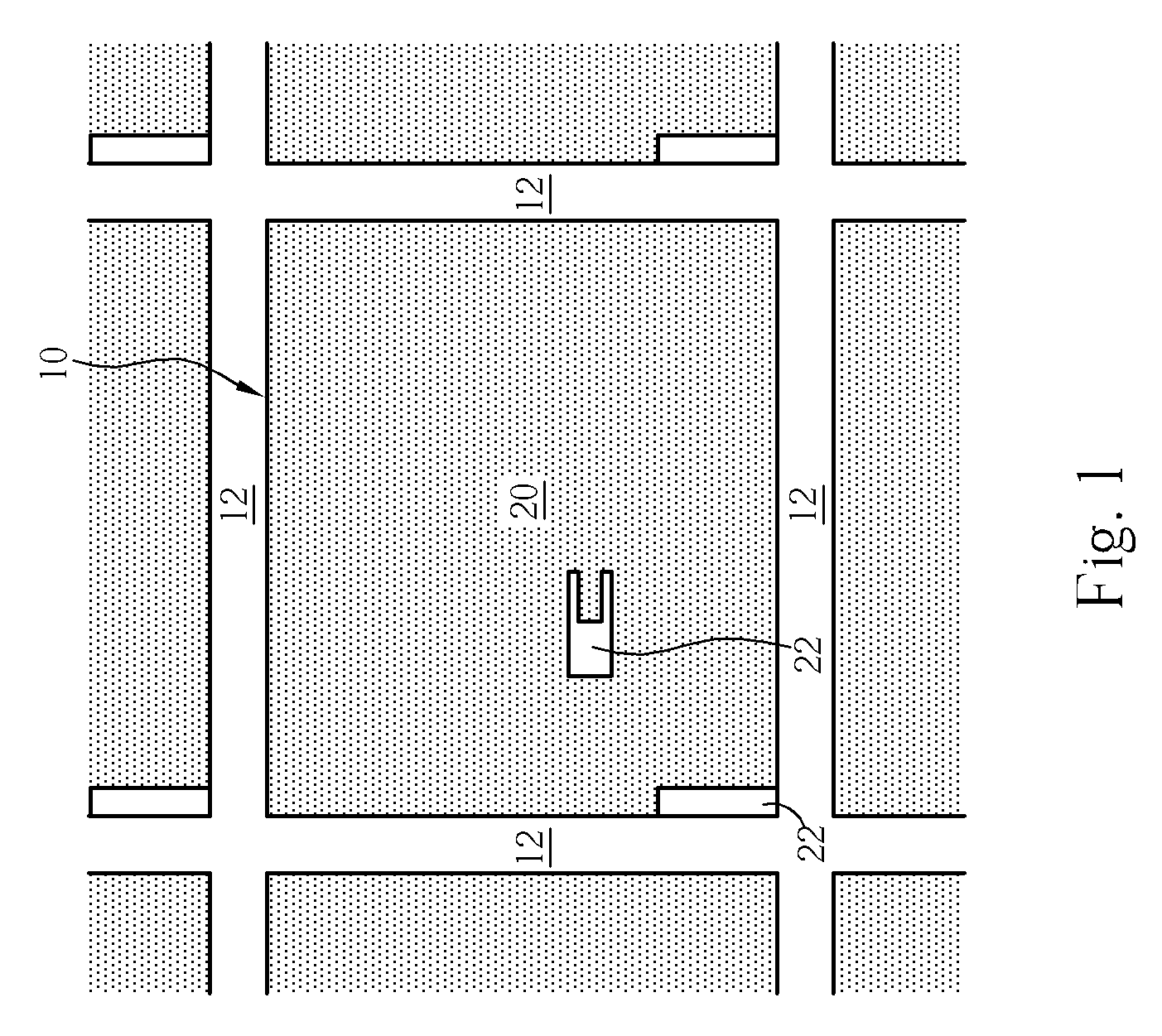
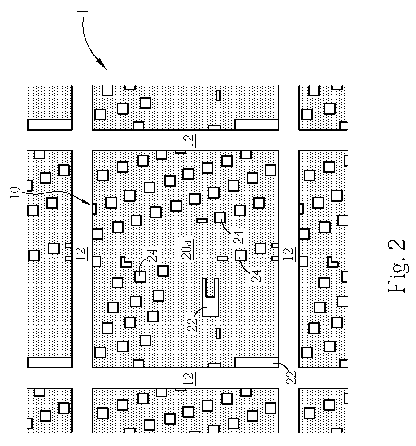
[0022]FIG. 1 is a schematic plan view of layout of a photoresist implant mask 20 for implementing lightly doped drain (LDD) regions of high-voltage devices in an integrated circuit die. As shown in FIG. 1, the integrated circui...


PUM


Abstract

A semiconductor substrate having an integrated circuit die area surrounded by a scribe lane is provided. Within the integrated circuit die area, a first trench isolation region and a second trench isolation region are formed on the semiconductor substrate, wherein the first trench isolation region isolates a first active device region from a second active device region, and the second trench isolation region comprises a plurality of trench dummy features for reducing loading effect. A first gate electrode is formed on the first active device region and a second gate electrode on the second active device region. The first active device region is masked, while the second active device region and the trench dummy features are exposed. An ion implantation process is then performed to implant dopant species into the second active device region.

Description

CROSS REFERENCE TO RELATED APPLICATIONS [0001] This is a continuation-in-part of U.S. patent application Ser. No. 10 / 908,815, filed May 27, 2005 and U.S. patent application Ser. No. 11 / 160,630, filed Jul. 1, 2005.BACKGROUND OF THE INVENTION [0002] 1. Field of the Invention [0003] The present invention relates generally to the field of semiconductor fabrication and, more particularly, to a method of reducing charging damage to integrated circuits during semiconductor manufacturing. The present invention is particularly suited for ion implant processing in an ion implanter without employing a plasma flood system. [0004] 2. Description of the Prior Art [0005] Ion implanters and ion implant process are commonly used in the manufacture of semiconductor products for implanting dopant species into wafers or semiconductor substrates to change the conductivity of the material in such substrates. Ion implanters generally comprise an ion source for generating a beam of ions, a mass analyzer fo...

Claims


Application Information

Patent Timeline
IPC IPC(8): H01L21/66
CPCH01L21/266H01L27/0207H01L21/823481H01L21/823418
Inventor CHANG, HSIEN-CHANGHOU, CHIA-HSINCHU, TSU-YUCHEN, KO-TING
Owner MARLIN SEMICON LTD
Why Eureka
Try Eureka