Method and apparatus for reducing charge density on a dielectric coated substrate after exposure to large area electron beam

Inactive Publication Date: 2005-10-13
APPLIED MATERIALS INC
View PDF20 Cites 5 Cited by
  • Summary
  • Abstract
  • Description
  • Claims
  • Application Information

AI Technical Summary

Benefits of technology

[0010] Embodiments in accordance with the present invention relate to a number of techniques, which may be applied alone or in combination, to reduce charge damage of substrates exposed to electron beam radiation. In accordance with one embodiment, charge damage may be reduced by establishing a robust electrical connection between the exposed substrate and ground. In accordance with another embodiment, charge damage may be reduced by modifying the sequence of steps for activating and deactivati

Problems solved by technology

As device sizes become smaller and integration density increases, one issue that has become an increasing concern to semiconductor manufacturers is that of inter-level “crosstalk.” Crosstalk is the undesired coupling of an electrical signal on one metal layer onto another metal layer, and arises when two or more layers of metal with intervening insulating or dielectric layers are formed on a substrate.
Undesired coupling of electrical signals can also occur between adjacent conductive traces, or lines, within a condu

Method used


Image

  • Method and apparatus for reducing charge density on a dielectric coated substrate after exposure to large area electron beam
  • Method and apparatus for reducing charge density on a dielectric coated substrate after exposure to large area electron beam
  • Method and apparatus for reducing charge density on a dielectric coated substrate after exposure to large area electron beam

Examples


Example

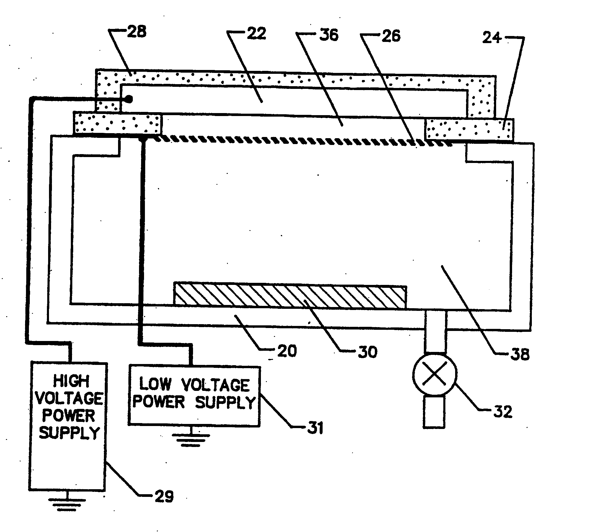
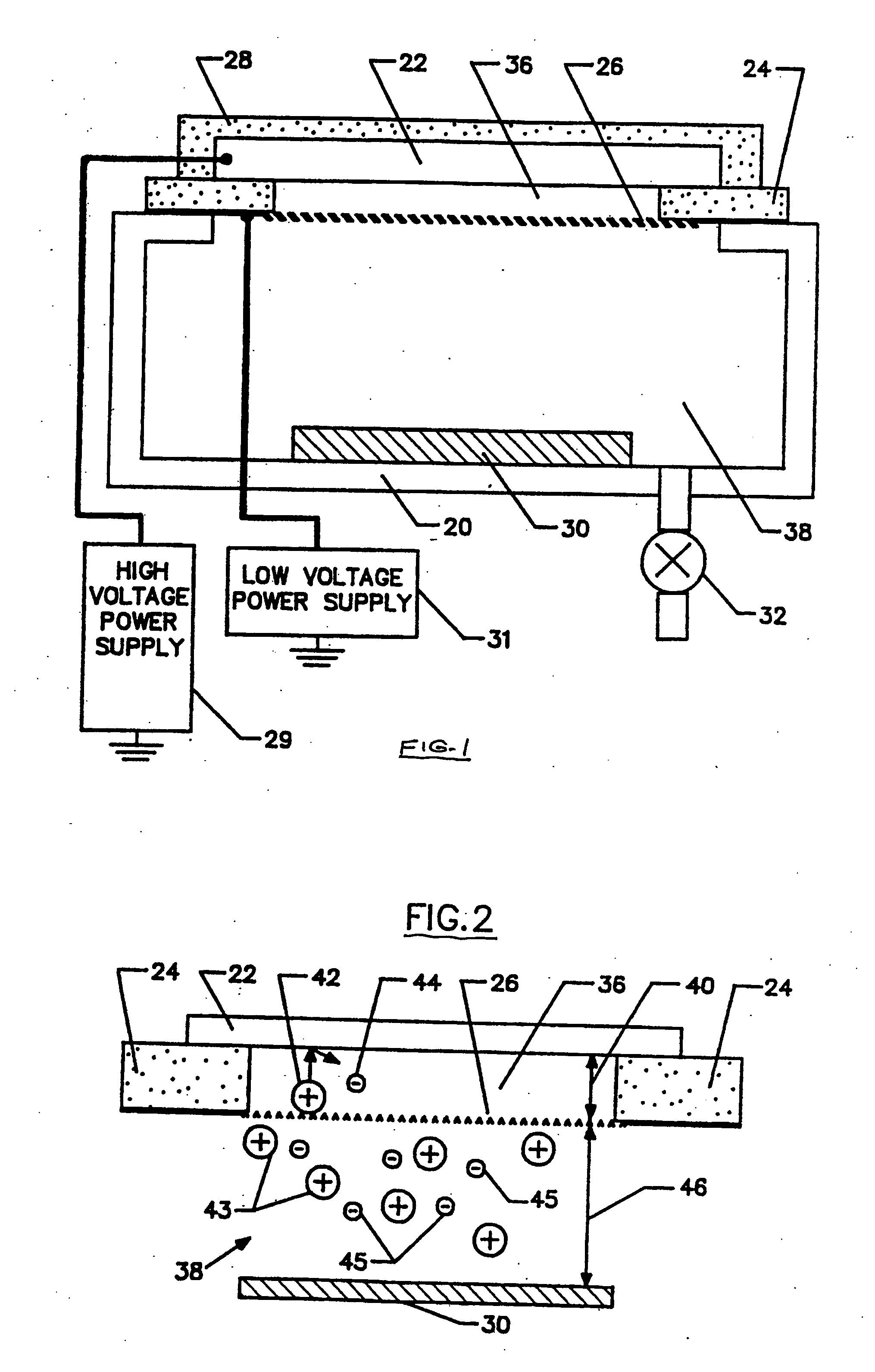
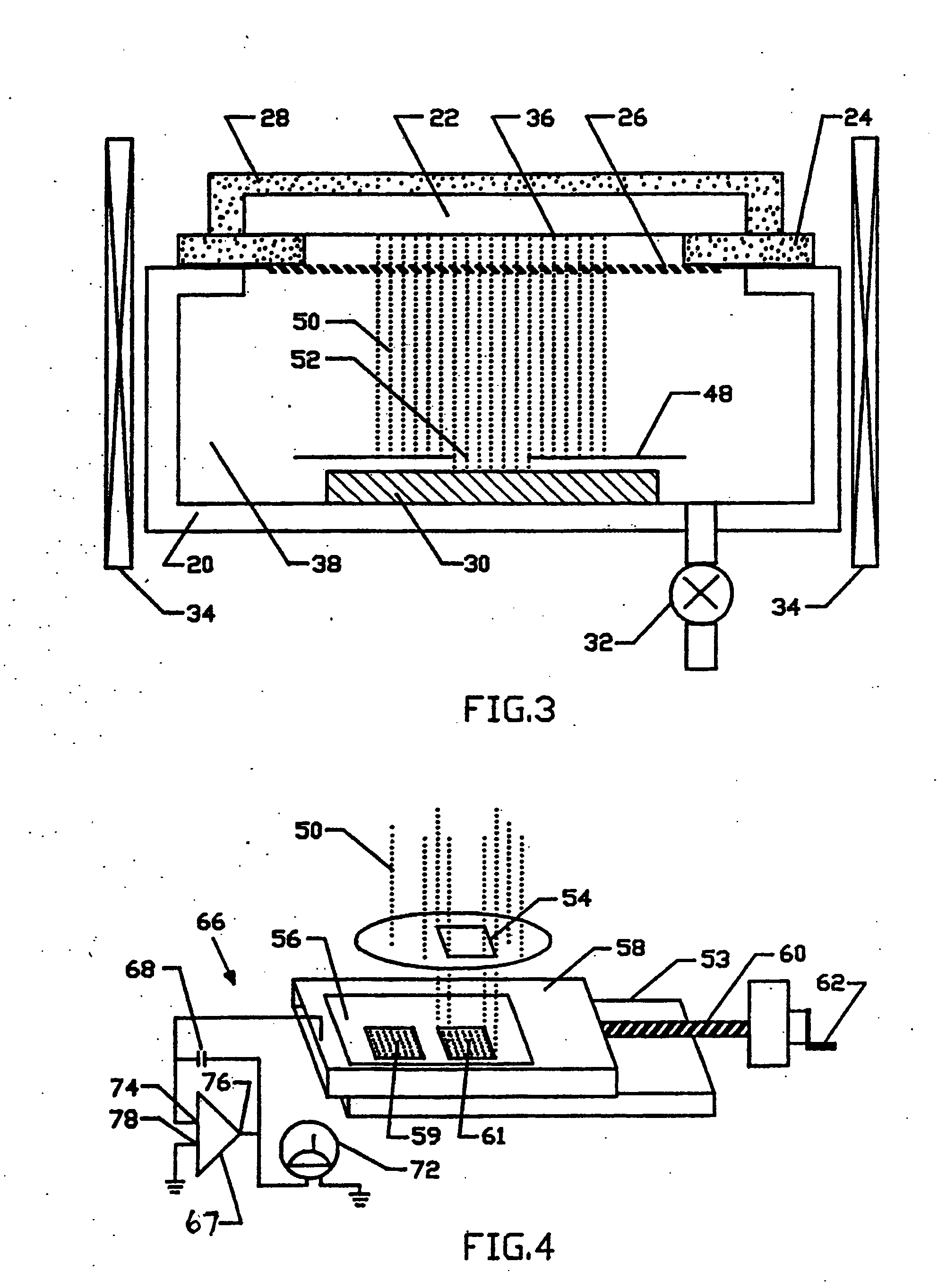
[0032] Embodiments of the present invention relate generally to semiconductor processing. Particular embodiments provide a method and structure to control charge buildup in dielectric films. Merely by way of example, the invention has been applied to reducing charge buildup in dielectric films after exposure to radiation from a large area electron beam. The method and structure can be applied to other applications including, but not limited to, the control of charge buildup in other materials, such as semiconductor materials, composite semiconductor / dielectric materials, and the like.

[0033] U.S. Pat. No. 5,003,178, incorporated herein by reference for all purposes, describes a design for a large-area uniform electron source. The following additional U.S. patents, describing various applications for electron beam processing, are also incorporated hereby by reference: U.S. Pat. No. 5,468,595, U.S. Pat. No. 6,132,814, U.S. Pat. No. 6,204,201, U.S. Pat. No. 6,207,555, U.S. Pat. No. 6,2...


PUM


Abstract

Embodiments in accordance with the present invention relate to a number of techniques, which may be applied alone or in combination, to reduce charge damage of substrates exposed to electron beam radiation. In one embodiment, charge damage is reduced by establishing a robust electrical connection between the exposed substrate and ground. In another embodiment, charge damage is reduced by modifying the sequence of steps for activating and deactivating the electron beam source to reduce the accumulation of charge on the substrate. In still another embodiment, a plasma is struck in the chamber containing the e-beam treated substrate, thereby removing accumulated charge from the substrate. In a further embodiment of the present invention, the voltage of the anode of the e-beam source is reduced in magnitude to account for differences in electron conversion efficiency exhibited by different cathode materials.

Description

CROSS-REFERENCES TO RELATED APPLICATIONS [0001] This application is a non-provisional application of and claims the benefit of U.S. Provisional Application No. 60 / 558,009, filed on Mar. 30, 2004, which is herein incorporated by reference in its entirety for all purposes.BACKGROUND OF THE INVENTION [0002] Semiconductor device geometries have dramatically decreased in size since integrated circuits were first introduced several decades ago, and all indications are that this trend will continue on. Today's wafer fabrication plants are routinely producing devices having 0.25 μm and even 0.18 μm feature sizes, and the plants of the future will soon be producing devices having even smaller geometries. [0003] As device sizes become smaller and integration density increases, one issue that has become an increasing concern to semiconductor manufacturers is that of inter-level “crosstalk.” Crosstalk is the undesired coupling of an electrical signal on one metal layer onto another metal layer,...

Claims


Application Information

Patent Timeline
IPC IPC(8): H01J37/317
CPCH01J37/317H01J2237/0041
Inventor DEMOS, ALEXANDROS T.ELSHEREF, KHALED A.TRACHUK, YURICHO, TOM K.DIXIT, GIRISH A.M'SAAD, HICHEMWITTY, DEREK
Owner APPLIED MATERIALS INC
Why Eureka
Try Eureka