

Photosensitive solder resist ink and preparation method thereof, printed circuit board and electronic equipment
A technology of photosensitive solder resist ink and polymerization inhibitor, which is applied in the fields of printed circuit, optomechanical equipment, printed circuit manufacturing, etc. It can solve the problems of easy charge accumulation, difficult PCB effective heat dissipation, electromigration, etc., and achieve excellent antistatic performance , Excellent heat dissipation capacity, the effect of excellent thermal conductivity
- Summary
- Abstract
- Description
- Claims
- Application Information
AI Technical Summary
Problems solved by technology
Method used
Image

Examples
preparation example Construction
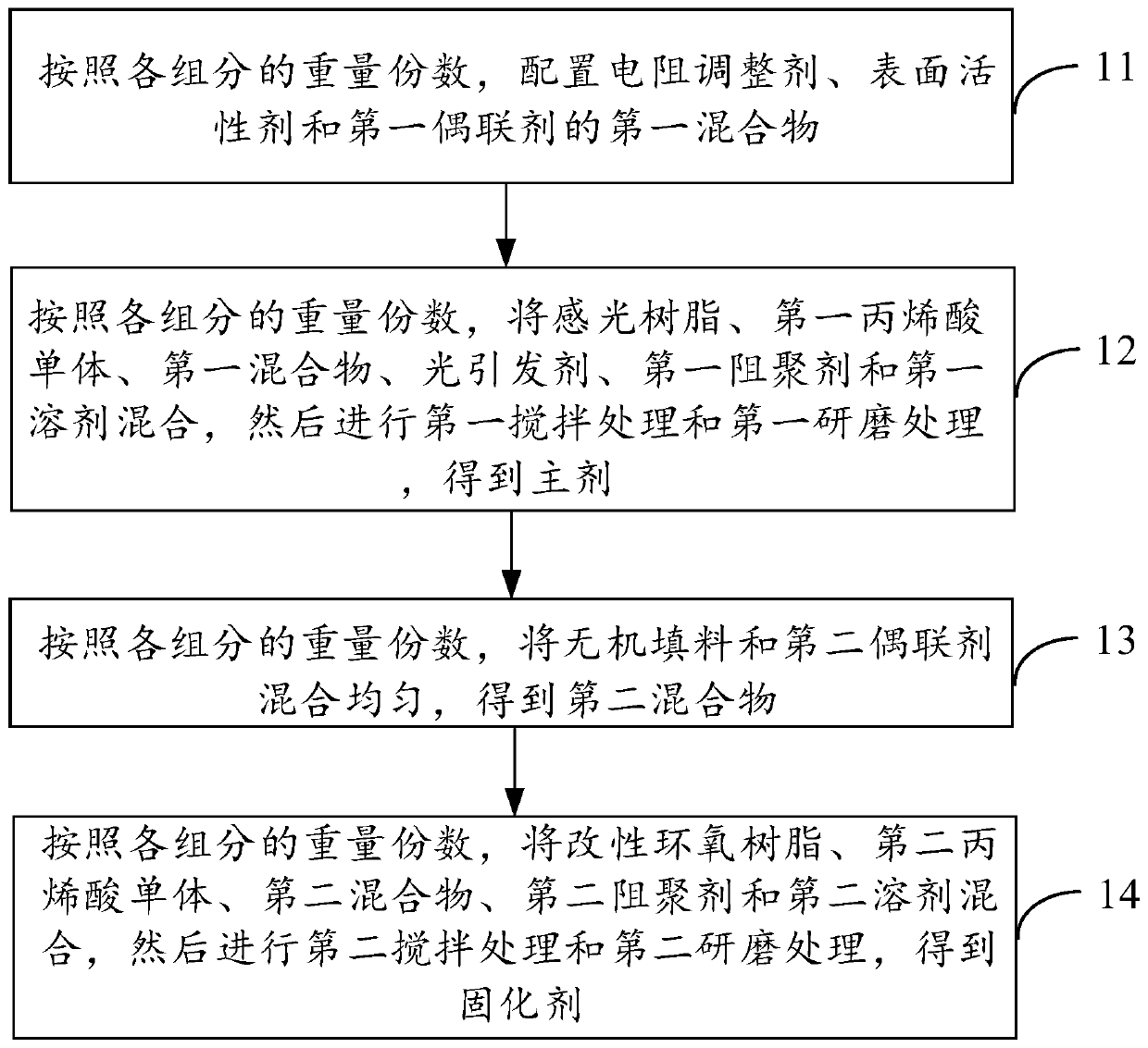
[0059] figure 1 Shown is a flowchart of a method for preparing a photosensitive solder resist ink according to an exemplary embodiment of the present disclosure. Some embodiments of the present disclosure also provide a preparation method of any photosensitive solder resist ink mentioned above, refer to figure 1 , the preparation method of photosensitive solder resist ink comprises:
[0060] Step 11. Prepare the first mixture of the resistance adjusting agent, the surfactant and the first coupling agent according to the parts by weight of each component.
[0061] Wherein, the first coupling agent can improve the interfacial performance between the resistance adjusting agent and other components, and the resistance adjusting agent can be uniformly dispersed in the first mixture through the coordination of the first coupling agent and the surfactant.
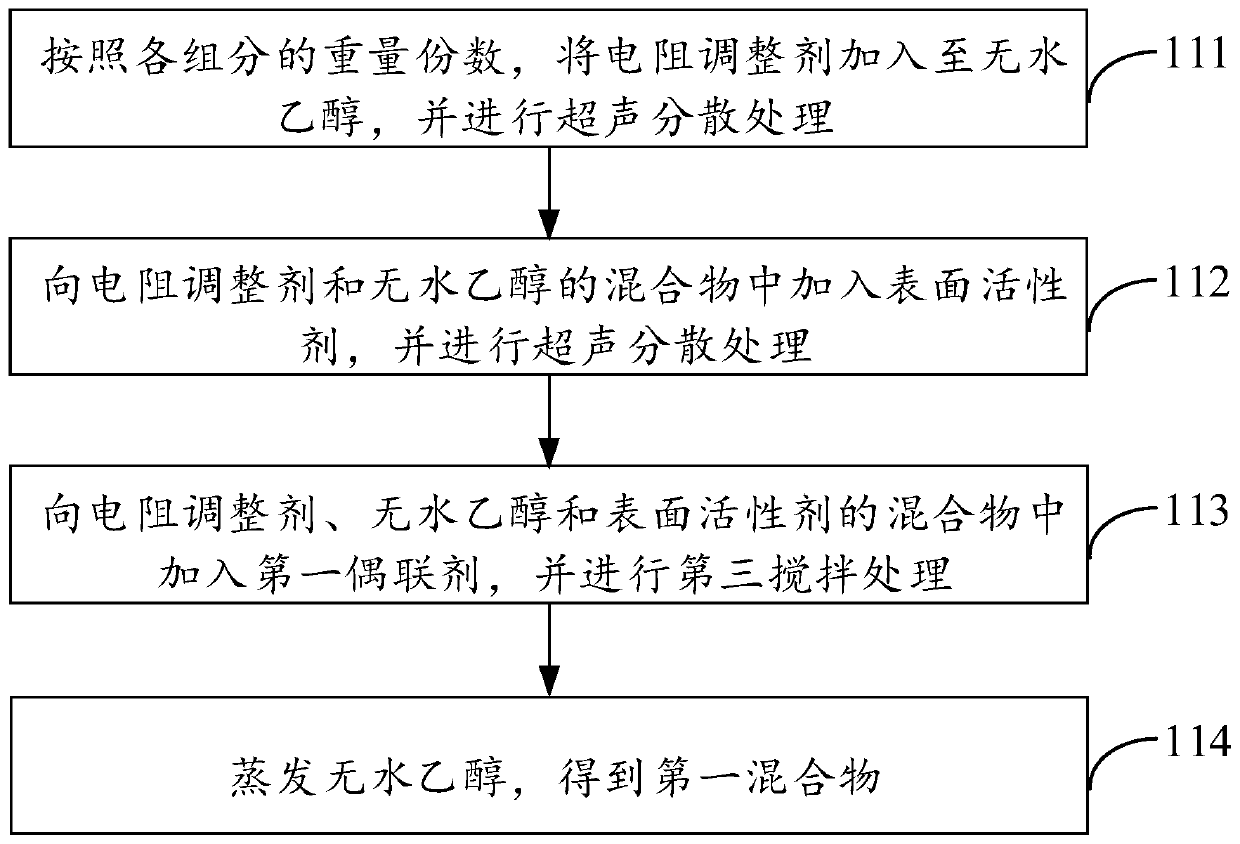
[0062] figure 2 Shown is a flowchart of a method for configuring a first mixture according to an exemplary embodiment of the...
Embodiment 1
[0085] This embodiment provides a photosensitive solder resist ink, the preparation method of which comprises:
[0086] According to the parts by weight of each component, 2 parts of conductive carbon black and 2 parts of short carbon nanotubes are mixed, then added into absolute ethanol, and subjected to ultrasonic dispersion treatment. Add 0.5 parts of sodium dodecylbenzenesulfonate to the mixture of conductive carbon black, short carbon nanotubes and absolute ethanol, and perform ultrasonic dispersion treatment. The power of ultrasonic dispersion treatment is 400W, and the temperature is 30°C. Add 2 parts of silane coupling agent KH550 to the mixture of conductive carbon black, short carbon nanotubes, absolute ethanol and sodium dodecylbenzenesulfonate, and stir for 2 hours at a stirring speed of 400 rpm to obtain the first mixture.
[0087] 80 parts of photosensitive resin, 12 parts of the first acrylic monomer, 2 parts of the first mixture, 8 parts of photoinitiator 784, ...
Embodiment 2
[0092] This embodiment provides a photosensitive solder resist ink, the preparation method of which comprises:
[0093] According to the parts by weight of each component, 5 parts of conductive carbon black were added into absolute ethanol, and subjected to ultrasonic dispersion treatment. Add 0.5 parts of sodium dodecylbenzenesulfonate to the mixture of conductive carbon black and absolute ethanol, and perform ultrasonic dispersion treatment, the power of ultrasonic dispersion treatment is 400W, and the temperature is 30°C. Add 1.5 parts of silane coupling agent KH570 to the mixture of conductive carbon black, absolute ethanol and sodium dodecylbenzenesulfonate, and stir at a stirring speed of 400 rpm for 3 hours to obtain the first mixture.
[0094] 100 parts of photosensitive resin, 16 parts of the first acrylic monomer, 3 parts of the first mixture, 10 parts of photoinitiator 819, 1 part of polydimethylsiloxane, 0.2 parts of leveling agent, 0.1 part of the first polymeriza...
PUM
| Property | Measurement | Unit |
|---|---|---|
| Viscosity | aaaaa | aaaaa |
Abstract
Description
Claims
Application Information