

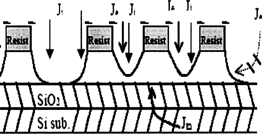
Polysilicon etching technology capable of preventing device from plasma damage
A technology of plasma and polysilicon, which is applied in semiconductor/solid-state device manufacturing, electrical components, circuits, etc., can solve the problems of process window and process results, and cannot solve the problems of silicon wafer damage, so as to reduce plasma damage and avoid charge accumulation , the effect of optimizing the design
- Summary
- Abstract
- Description
- Claims
- Application Information
AI Technical Summary
Problems solved by technology
Method used
Image

Examples
Embodiment 1
[0026] In the etching process, the silicon wafer is first introduced into the etching reaction chamber, which is adsorbed and fixed by the electrostatic chuck. The temperature of the chamber is controlled at 60°C, and the temperature of the silicon wafer temperature control system is set at 60°C. To improve the temperature uniformity, add The pressure of the He gas back blowing system is set to 8T, and the etching process is performed after the auxiliary process conditions are stable.
[0027] BT step etching: chamber pressure 7mT, upper RF power supply 300W, lower RF power supply 40W, process gas CF 4 The flow rate is 50sccm, and the process time is 5s.
[0028] Main step etching: chamber pressure 10mT, upper RF power 350W, lower RF power 40W, process gas Cl 2 30sccm, HBr 170sccm, HeO 2 (The volume ratio of the two is 7:3, the same below) 15sccm mixed gas, the process time control is detected and controlled by the end point detection system.
[0029] Step etching: chamber...
Embodiment 2
[0032] Using the method of Example 1, the difference is that a stop step is added after the main step, and the specific process is as follows: the swing valve is fully opened, the power of the upper and lower electrodes is 0w, the gas flow rate is 0sccm, and the time is 30s.
[0033] In addition, the specific process of the silicon wafer unloading step is as follows: the chamber pressure is 15mT, the power of the upper electrode is 300W (turn off in ramp mode for 2s), the power of the lower electrode is 0W, the flow rate of the process gas Ar is 200sccm, and the process time is 5s.
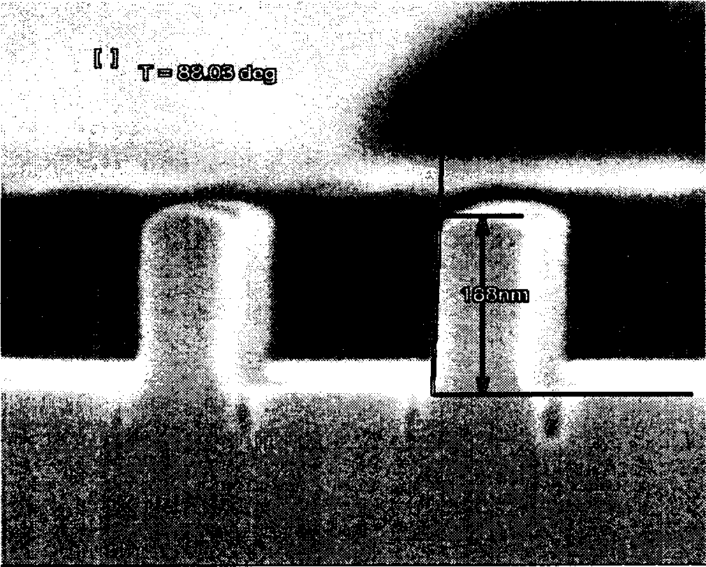
[0034] FE-SEM slicing results see image 3 As shown, no microtrench phenomenon was found, indicating that the potential plasma damage was significantly improved.
Embodiment 3
[0036] Using the method of Example 2, the difference is that a stop step is added after the main step, and the specific process is as follows: the swing valve is fully opened, the power of the upper and lower electrodes is 0w, the gas flow rate is 0sccm, and the time is 300s. Wherein the specific process of silicon wafer unloading step is: chamber pressure 10mT, upper electrode power 200W (using ramp mode 5s off), lower electrode power 0W, process gas O 2 The flow rate is 300sccm, and the process time is 5s.
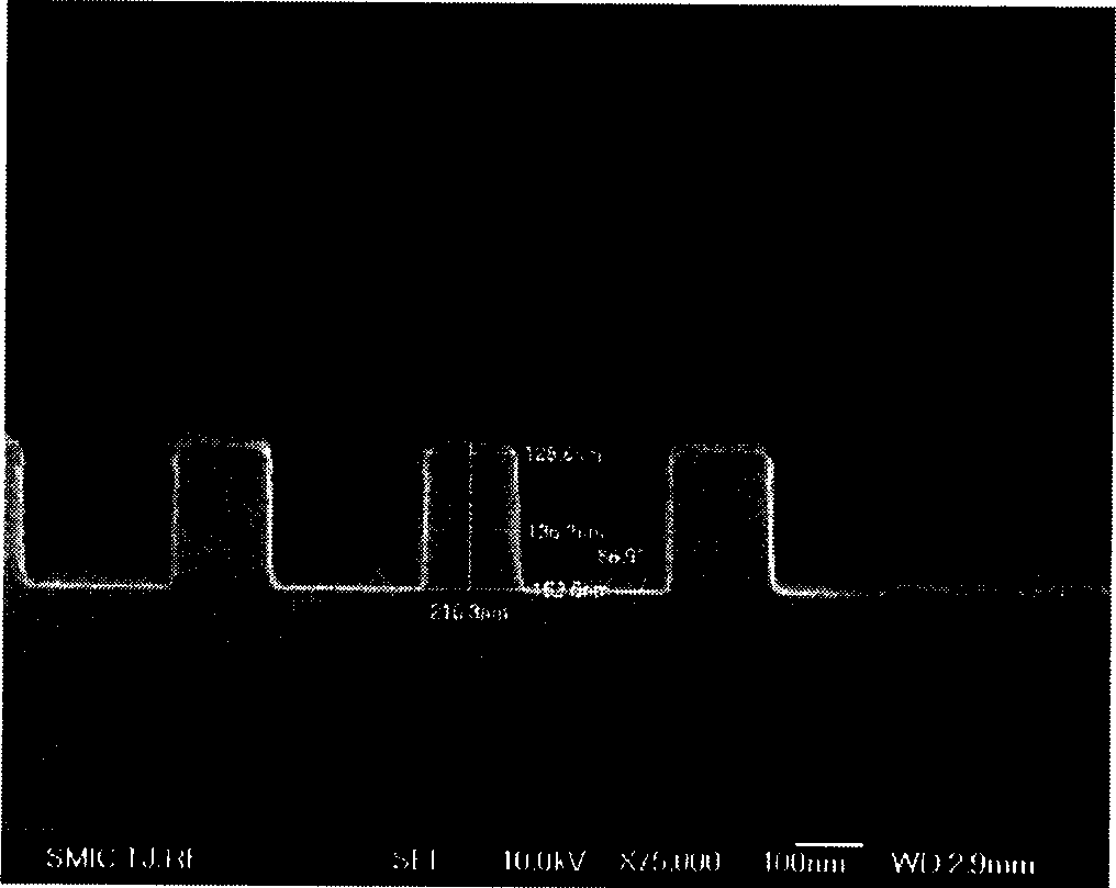
[0037] FE-SEM results see Figure 4 As shown, no microchannel phenomenon was found.
PUM
 Abstract
Description
Claims
Application Information