Semiconductor package and manufacturing method thereof

a technology of semiconductors and packaging, applied in the direction of semiconductor devices, semiconductor/solid-state device details, electrical apparatus, etc., can solve the problems of high internal pressure, easy damage to the connection portion, and damage to the molding part, and achieve excellent electromagnetic interference (emi) and electromagnetic susceptibility characteristics

Inactive Publication Date: 2012-05-03
SAMSUNG ELECTRO MECHANICS CO LTD
View PDF6 Cites 35 Cited by
  • Summary
  • Abstract
  • Description
  • Claims
  • Application Information

AI Technical Summary

Benefits of technology

[0012]An aspect of the present invention provides a semiconductor package including an electromagnetic shielding structure having excellent electromagnetic interference (EMI

Problems solved by technology

At this time, a connection portion between the ground pattern of the substrate and the shield is formed to have a very fine pattern, whereby the connection portion may be easily damaged due to external impacts, or the like.
When the semiconductor package passes through an oven at a high temperature in the state in which the fill

Method used


Image

  • Semiconductor package and manufacturing method thereof
  • Semiconductor package and manufacturing method thereof
  • Semiconductor package and manufacturing method thereof

Examples


Embodiment Construction

[0038]The terms and words used in the present specification and claims should not be interpreted as being limited to typical meanings or dictionary definitions, but should be interpreted as having meanings and concepts relevant to the technical scope of the present invention based on the rule according to which an inventor can appropriately define the concept of the term to describe most appropriately the best method he or she knows for carrying out the invention. Therefore, the configurations described in the embodiments and drawings of the present invention are merely most preferable embodiments but do not represent all of the technical spirit of the present invention. Thus, the present invention should be construed as including all the changes, equivalents, and substitutions included in the spirit and scope of the present invention at the time of filing this application.

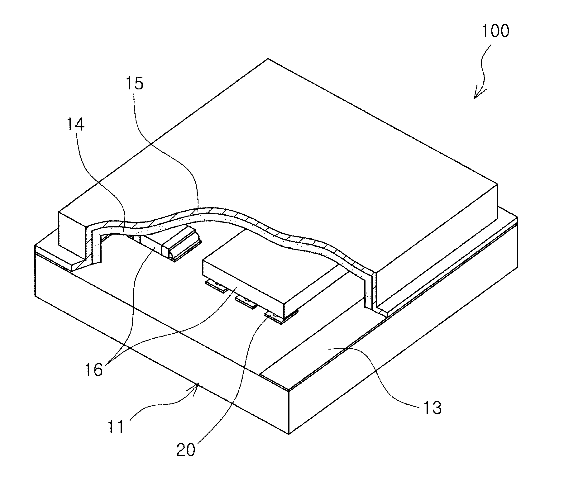
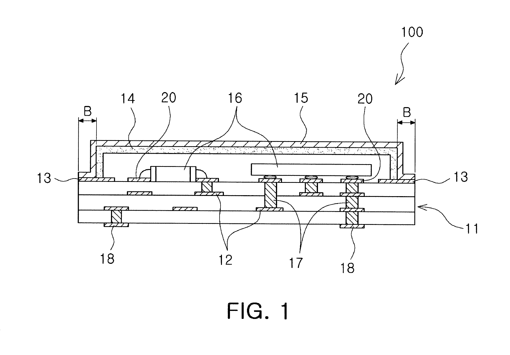
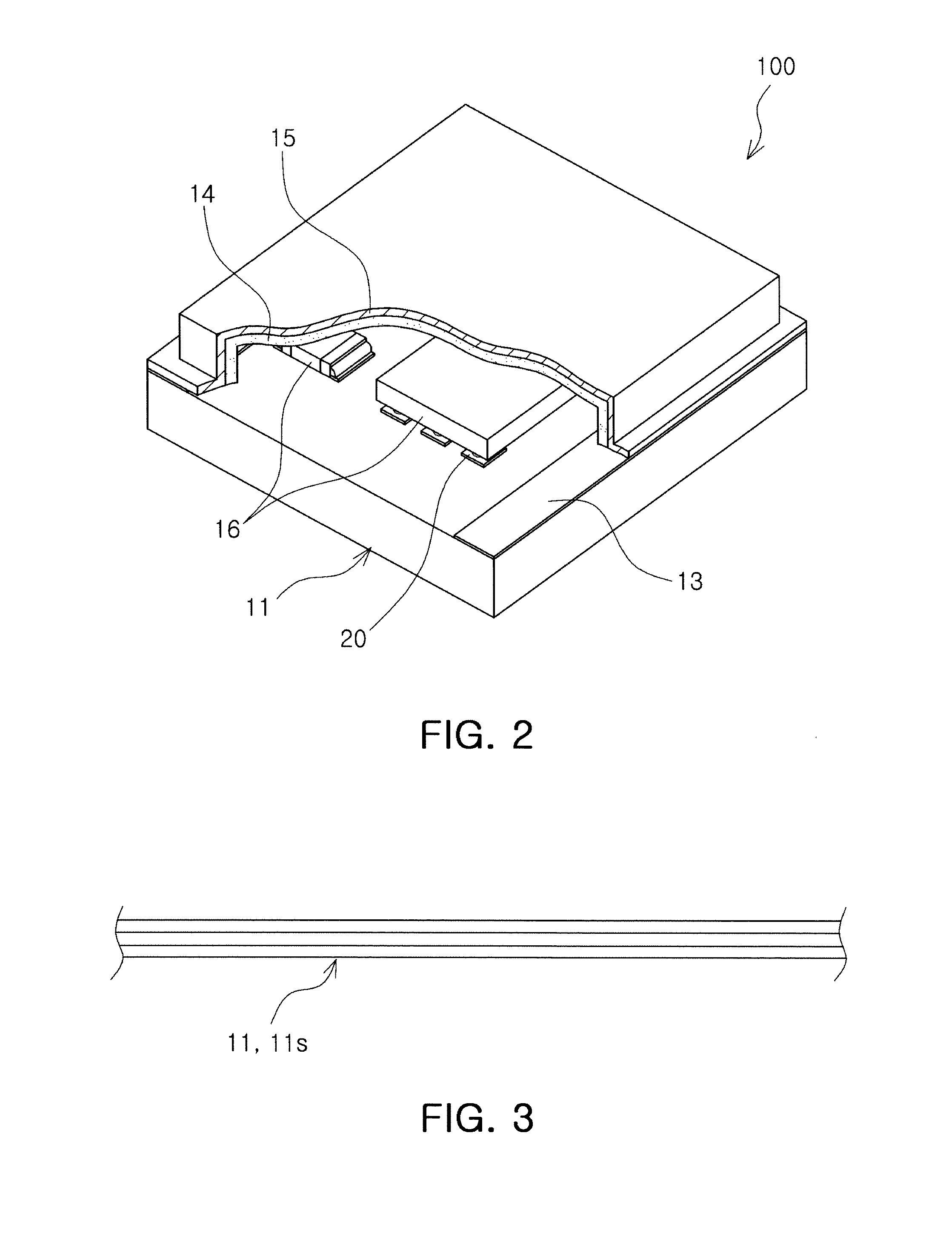
[0039]Hereinafter, exemplary embodiments of the present invention will be described in detail with reference to...


PUM


Abstract

There are provided a semiconductor package including an electromagnetic shielding structure having excellent electromagnetic interference (EMI) and electromagnetic susceptibility (EMS) characteristics, while protecting individual elements in an inner portion thereof from impacts, and a manufacturing method thereof. The semiconductor package includes: a substrate having ground electrodes formed on an upper surface thereof; at least one electronic component mounted on the upper surface of the substrate; an insulating molding part including an internal space in which the electronic component is accommodated, and fixed to the substrate such that at least a portion of the ground electrode is externally exposed; and a conductive shield part closely adhered to the molding part to cover an outer surface of the molding part and electrically connected to the externally exposed ground electrodes.

Description

CROSS-REFERENCE TO RELATED APPLICATIONS[0001]This application claims the priority of Korean Patent Application No. 10-2010-0105384 filed on Oct. 27, 2010, in the Korean Intellectual Property Office, the disclosure of which is incorporated herein by reference.BACKGROUND OF THE INVENTION[0002]1. Field of the Invention[0003]The present invention relates to a semiconductor package module and a manufacturing method thereof, and more particularly, to a semiconductor package module including a shielding member capable of shielding electromagnetic waves, while simultaneously protecting a passive element, a semiconductor chip, or the like, included in a package, from an external environment, and a manufacturing method thereof.[0004]2. Description of the Related Art[0005]In accordance with a recent rapid increase in market demand for portable electronic apparatuses, the demand for the miniaturization and lightness of electronic components mounted in these products has accordingly continuously...

Claims


Application Information

Patent Timeline
IPC IPC(8): H01L23/552H01L21/78
CPCH01L2224/16227H01L24/16H01L2924/01005H01L23/552H01L2924/16251H01L2924/1616H01L21/52H01L2924/1679H01L2224/16225H01L21/82H01L23/053H01L2924/15313H01L2924/01047H01L2924/16153H01L23/585H01L2224/97H01L24/97H01L2924/01033H01L2224/81H01L2924/15787H01L2924/19105H01L2924/00014H01L2924/16152H01L2924/00H01L2224/0401
Inventor YOO, JIN O.
Owner SAMSUNG ELECTRO MECHANICS CO LTD
Why Eureka
Try Eureka