
Semiconductor device and control method thereof

Active Publication Date: 2012-05-10
LONGITUDE LICENSING LTD
View PDF4 Cites 3 Cited by
  • Summary
  • Abstract
  • Description
  • Claims
  • Application Information

AI Technical Summary

Benefits of technology

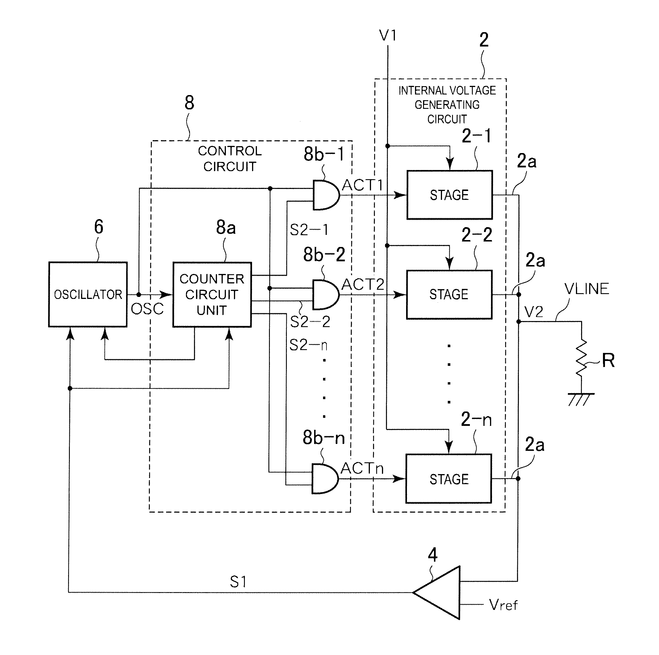
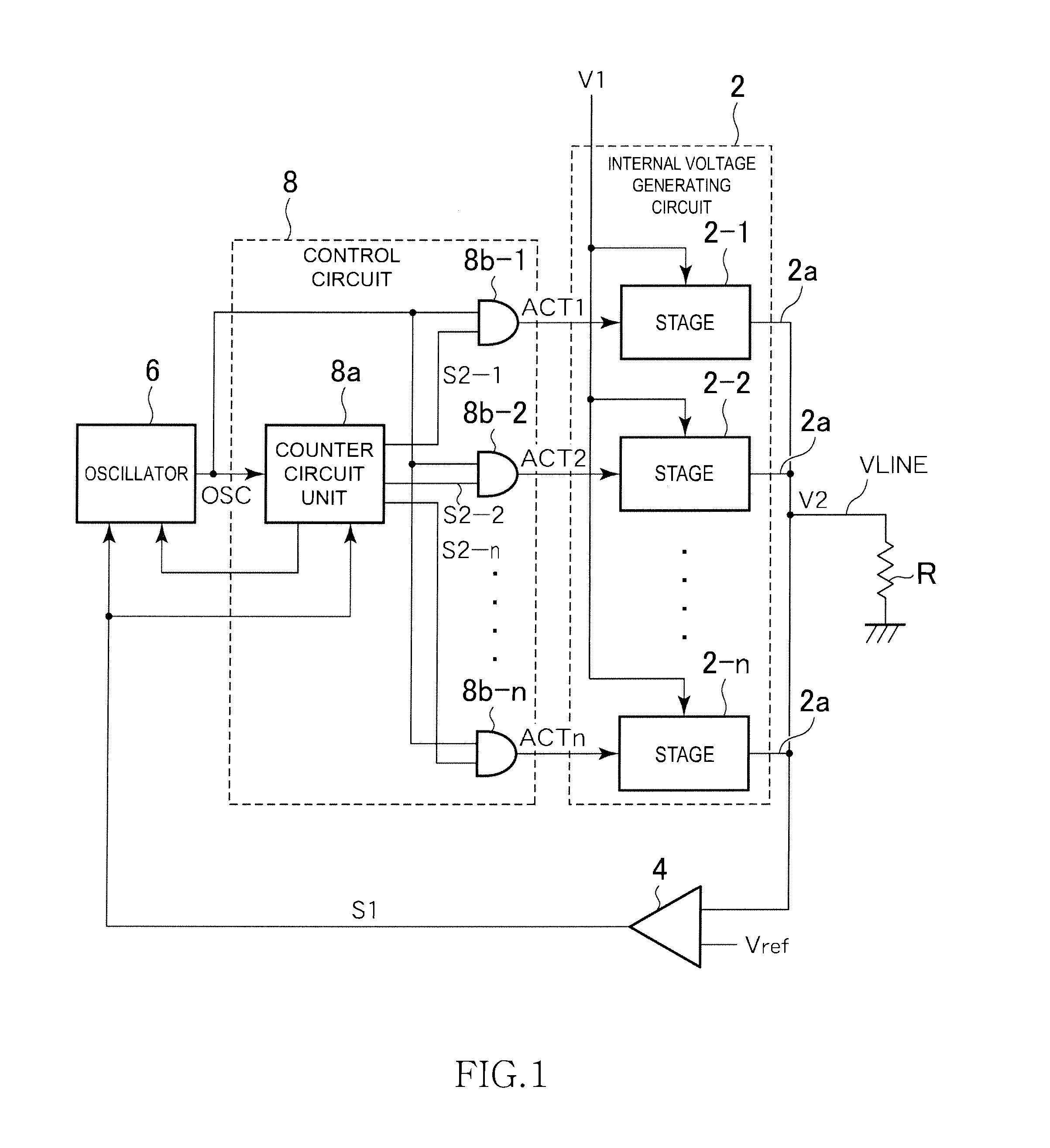
[0009]In another embodiment, there is provided a semiconductor device comprising: an internal voltage generating circuit that supplies a second voltage generated from a first voltage to an internal power supply line; a control circuit that controls the internal voltage generating circuit; and a first voltage detection circuit that detects a level of the first voltage, wherein the internal voltage generating circuit generates the second voltage regardless of the level of the first voltage, the control circuit stepwise increases an ability of generating the second voltage at a first speed when the internal voltage generating circuit is to be activated, the control circuit stepwise reduces the ability of generating the second voltage at a second speed when the internal voltage generating circuit is to be inactivated, the control circuit adjusts the first speed more slowly in increasing proximity of the level of the first voltage detected by the first voltage detection circuit to the second voltage, and the control circuit adjusts the second speed faster in increasing proximity of the level of the first voltage detected by the first voltage detection circuit to the second voltage.
[0011]According to the present invention, wild fluctuations of the internal voltage when an internal voltage generating circuit is activated or inactivated can be prevented.

Problems solved by technology

Therefore, when the internal voltage generating circuit is activated or inactivated, the internal voltage may fluctuate sharply, damaging stability of the internal voltage.
The above problems become particularly noticeable in a wide-range semiconductor device in which the range of the available external voltage is wide.
In a wide-range semiconductor device, it is unavoidable to design an internal voltage generating circuit by assuming a case when the level of the actually used external voltage is the lower limit of the available external voltage.
Thus, if the level of the actually used external voltage is, for example, the upper limit of the available external voltage, instead of the lower limit thereof, the voltage supply ability of the internal voltage generating circuit becomes excessive.
As a result, the internal voltage may fluctuate due to activation and inactivation of the internal voltage generating circuit.

Method used


Image

  • Semiconductor device and control method thereof
  • Semiconductor device and control method thereof
  • Semiconductor device and control method thereof

Examples


Embodiment Construction

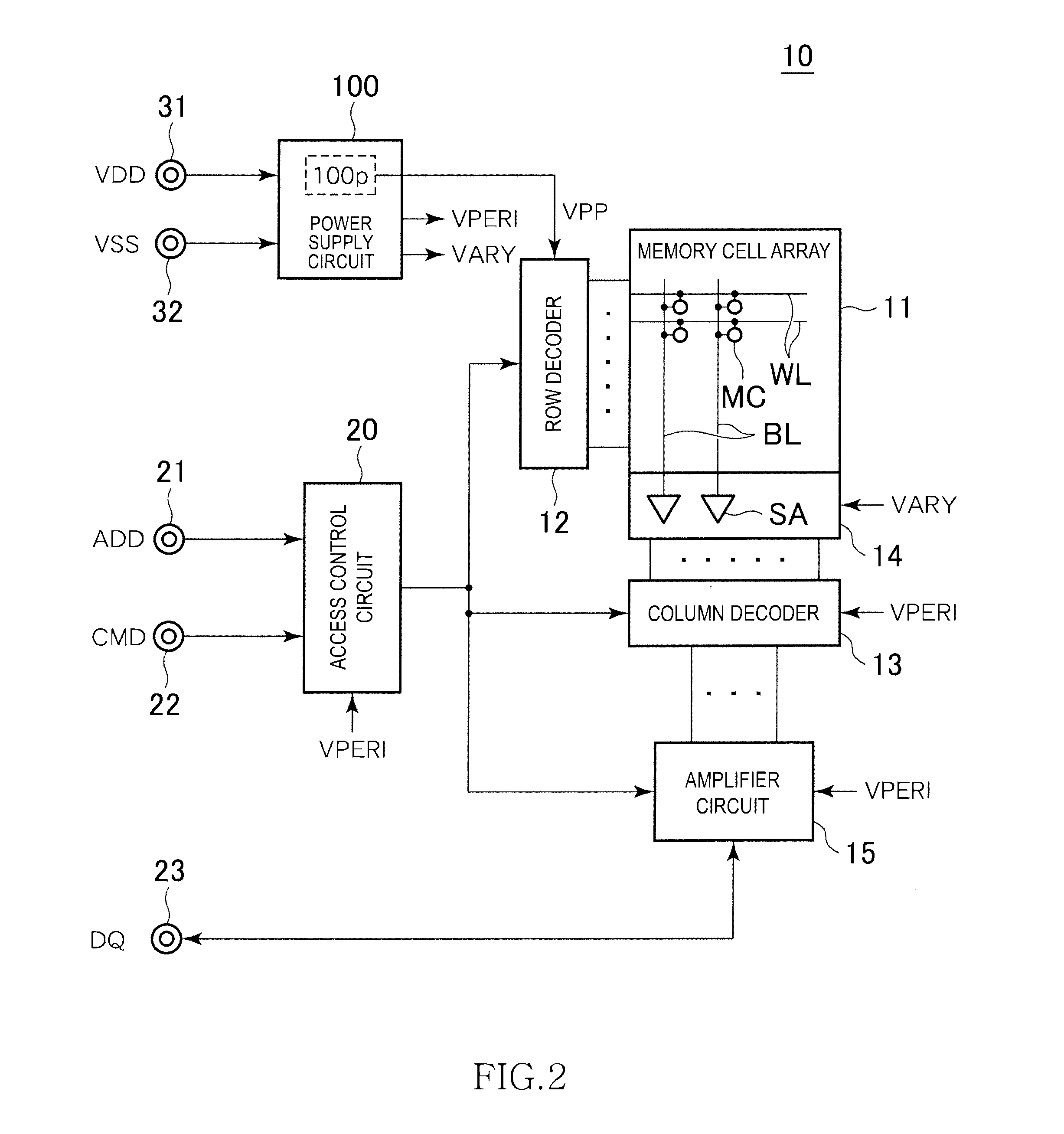
[0026]A representative example of the technical concept of the present invention will be described below. It will be understood that what is claimed by the present invention is not limited to such a technical concept and is set forth in the claims of the present invention. That is, the technical concept of the present invention is to generate a count value by counting an oscillator signal and to activate and inactivate a plurality of stages contained in an internal voltage generating circuit in response to mutually different count values. Activation and inactivation of the plurality of stages are each set independently of each other by different count values. Setting conditions thereof are also made different depending on the external voltage. That is, instead of sequentially activating a plurality of stages in first timing (first phase) simply by oscillator signals having different phases and sequentially inactivating the plurality of stages in the first timing (first phase), activ...


PUM


Abstract

Sharp fluctuations of an internal voltage when an internal voltage generating circuit is activated or inactivated are prevented. The internal voltage generating circuit to supply the internal voltage generated from an external voltage to an internal power supply line, a control circuit to control an operation of the internal voltage generating circuit, and a voltage detection circuit to detect a level of a first voltage are included. When, for example, the internal voltage generating circuit is activated, the control circuit stepwise increases supply ability of the internal voltage at a first speed and when the internal voltage generating circuit is inactivated, the control circuit stepwise reduces the supply ability of the internal voltage at a second speed that is different from the first speed. Accordingly, wild fluctuations of the internal voltage when the internal voltage generating circuit is activated / inactivated can optimally be prevented for each case.

Description

BACKGROUND OF THE INVENTION[0001]1. Field of the Invention[0002]The present invention relates to a semiconductor device and a control method thereof, and in particular, relates to a semiconductor device containing an internal voltage generating circuit and a control method thereof.[0003]2. Description of Related Art[0004]A semiconductor device such as a DRAM (Dynamic Random Access Memory) may contain a circuit operating based on an internal voltage that is different from an external voltage supplied from outside. In such a semiconductor device, an internal voltage generating circuit that generates an internal voltage based on an external voltage is provided (see Japanese Patent Application Laid-Open Nos. 2008-112507, 2000-306380, H2-156498, and 2004-147458).[0005]An internal voltage generating circuit described in Japanese Patent Application Laid-Open No. 2008-112507 or Japanese Patent Application Laid-Open No. 2000-306380 generates an internal voltage by operating a plurality of pa...

Claims


Application Information

Patent Timeline
IPC IPC(8): G05F1/10
CPCG11C5/145
Inventor YOSHIDA, KENJI
Owner LONGITUDE LICENSING LTD
Learn More