


Quick Research
Generate reliable direction feasibility study reports for your R&D in just a few steps.

Technical Q&A
Discover and master advanced knowledge NOW. Basics, ideas, possibilities, all at once.

Find Solutions
As an expert in R&D theories, this can generate solutions to your technical problems instantly.

Evaluate Feasibility
Analyze your overall solution with one click, know your potential R&D risks in advance.

Monitor Landscape
Get weekly tech updates, stay abreast of the latest tech innovations and key insights.
Integrated circuit packaging system with bump conductors and method of manufacture thereof
- Summary
- Abstract
- Description
- Claims
- Application Information
AI Technical Summary
Problems solved by technology
Method used
Image

Examples
first embodiment
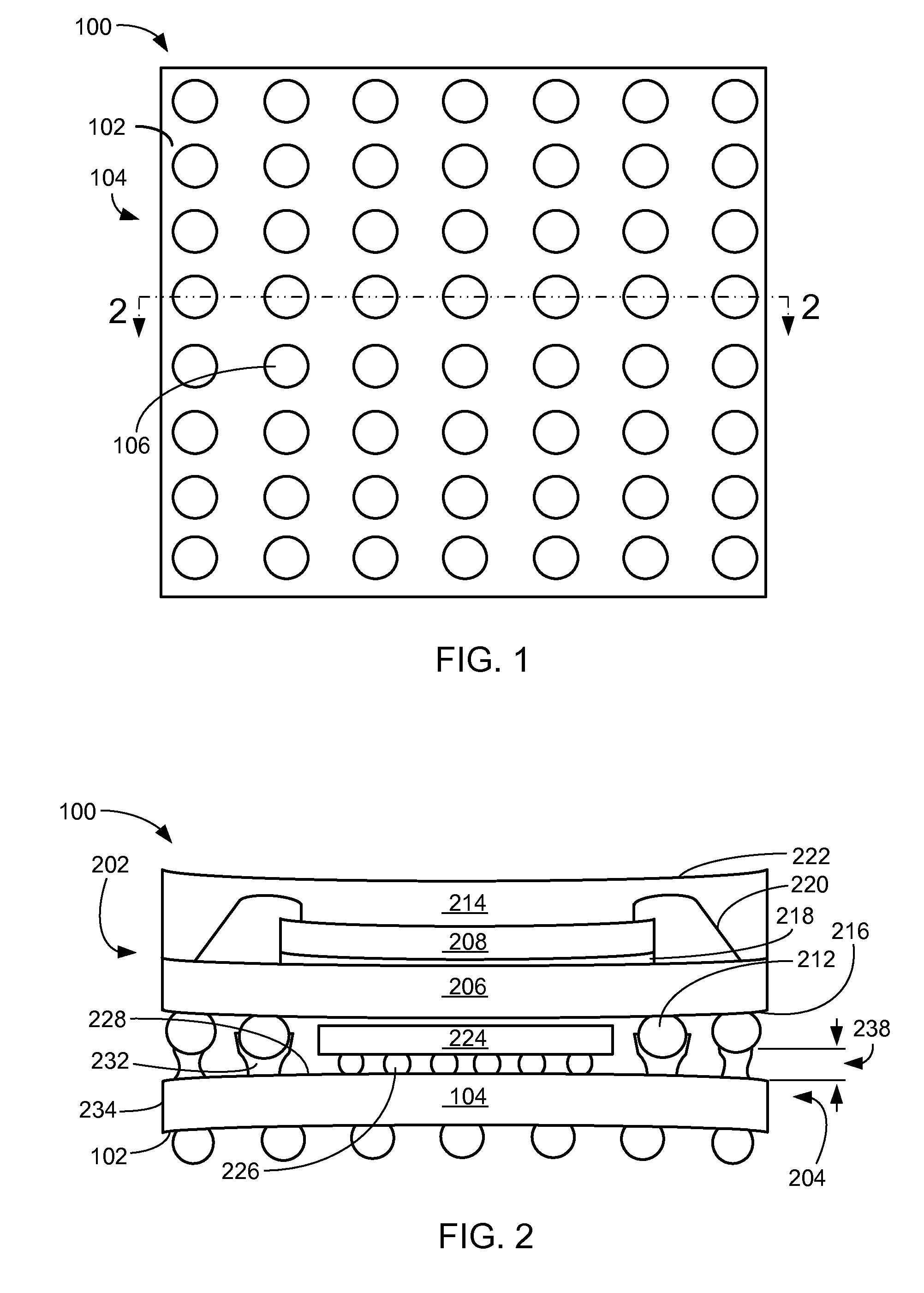
[0029]Referring now to FIG. 1, therein is shown a bottom view of an integrated circuit packaging system 100 in the present invention. Shown is a base side 102 of a base substrate 104 with system interconnects 106 on the base side 102.
[0030]The base substrate 104 can include a substrate, an interposer, a circuit board, or a laminate with base conductors. The base conductors are used to provide connectivity to areas on the base side 102, to areas on a side of the base substrate 104 opposite the base side 102, or between areas on the base side 102 and on the side of the base substrate 104 opposite the base side 102.
[0031]The system interconnects 106 can include conductive balls, bumps, pins, or pillars. The system interconnects 106 are attached to the base conductors on the base side 102 to provide connectivity the integrated circuit packaging system 100 and a next level of integration (not shown) that can include a printed circuit board, an integrated circuit module, or an electronic ...
second embodiment
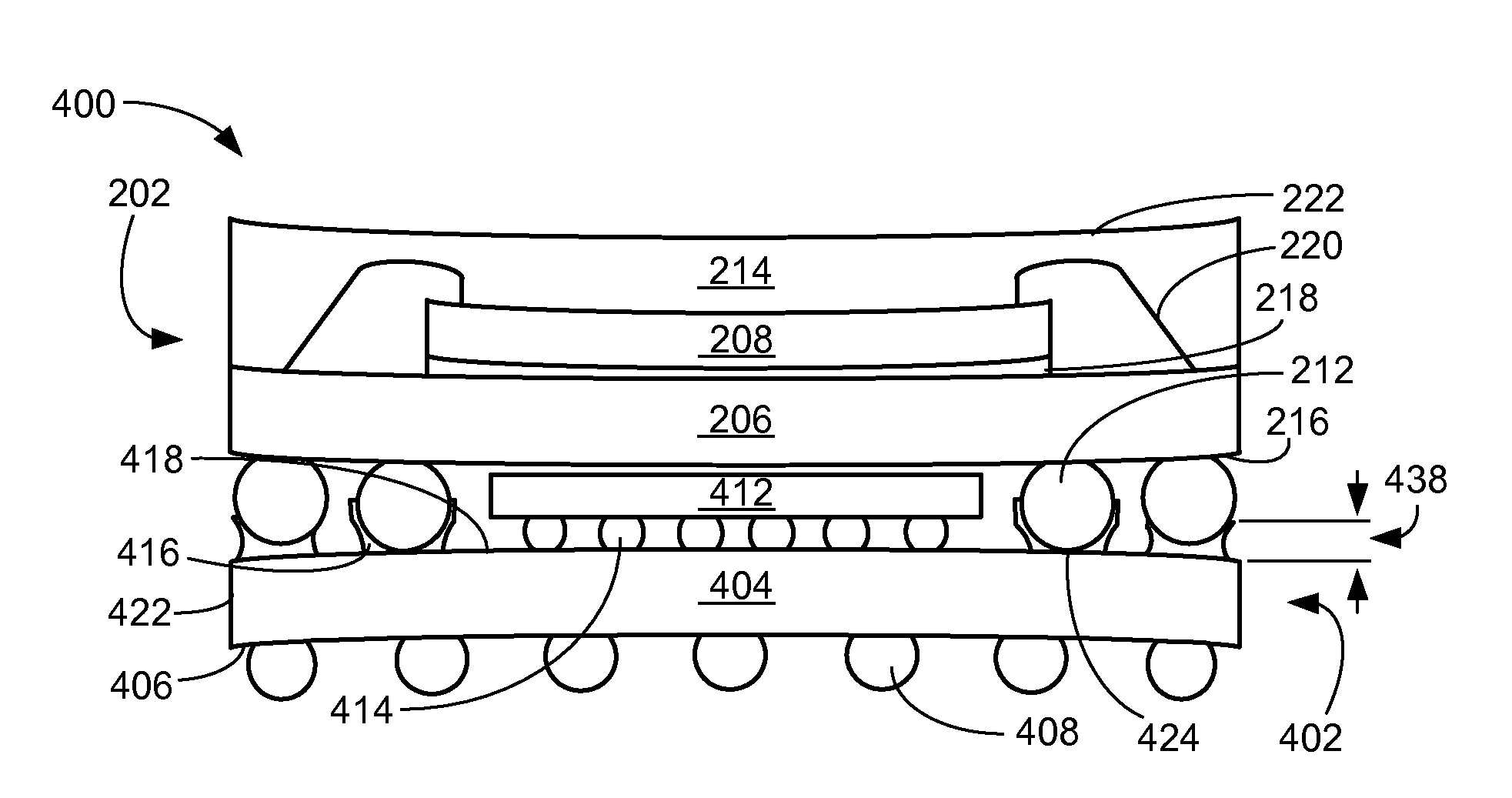
[0063]Referring now to FIG. 4, therein is shown a cross-sectional view of an integrated circuit packaging system 400 in the present invention. The integrated circuit packaging system 400 includes the stack package 202 over and connected or attached to a base package 402.
[0064]The stack package 202 includes the stack substrate 206, the stack device 208, the stack interconnects 212, and the stack encapsulation 214. The stack interconnects 212 are attached to the stack conductors on the stack side 216 of the stack substrate 206.
[0065]The stack device 208 can be mounted on the side of the stack substrate 206 opposite the stack side 216 using the stack attachment layer 218. The stack circuit connectors 220 are attached to circuitry of the stack device 208 and the stack conductors on the side of the stack substrate 206 opposite the stack side 216.
[0066]The stack encapsulation 214 covers the side of the stack substrate 206 opposite the stack side 216, the stack device 208, and the stack ci...
PUM
 Abstract
Description
Claims
Application Information
 - R&D Engineer
- R&D Manager
- IP Professional
- Industry Leading Data Capabilities
- Powerful AI technology
- Patent DNA Extraction
Browse by: Latest US Patents, China's latest patents, Technical Efficacy Thesaurus, Application Domain, Technology Topic, Popular Technical Reports.
© 2024 PatSnap. All rights reserved.Legal|Privacy policy|Modern Slavery Act Transparency Statement|Sitemap|About US| Contact US: help@patsnap.com