Socket and semiconductor device provided with socket
- Summary
- Abstract
- Description
- Claims
- Application Information
AI Technical Summary
Benefits of technology
Problems solved by technology
Method used
Image

Examples
embodiment 1
Configuration of Socket According to Embodiment 1
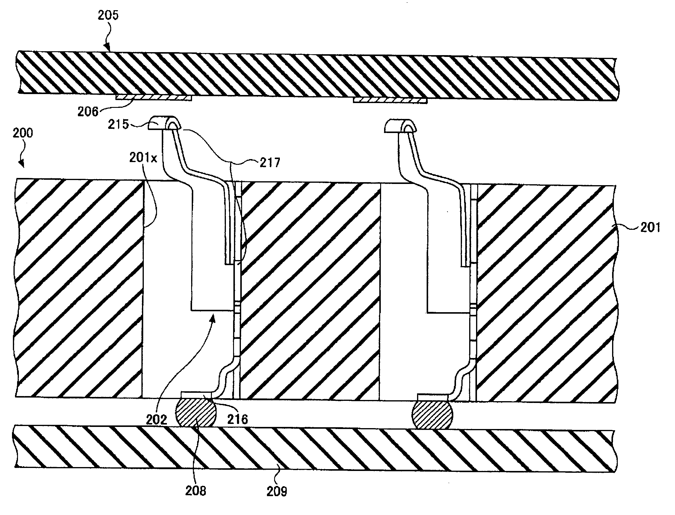
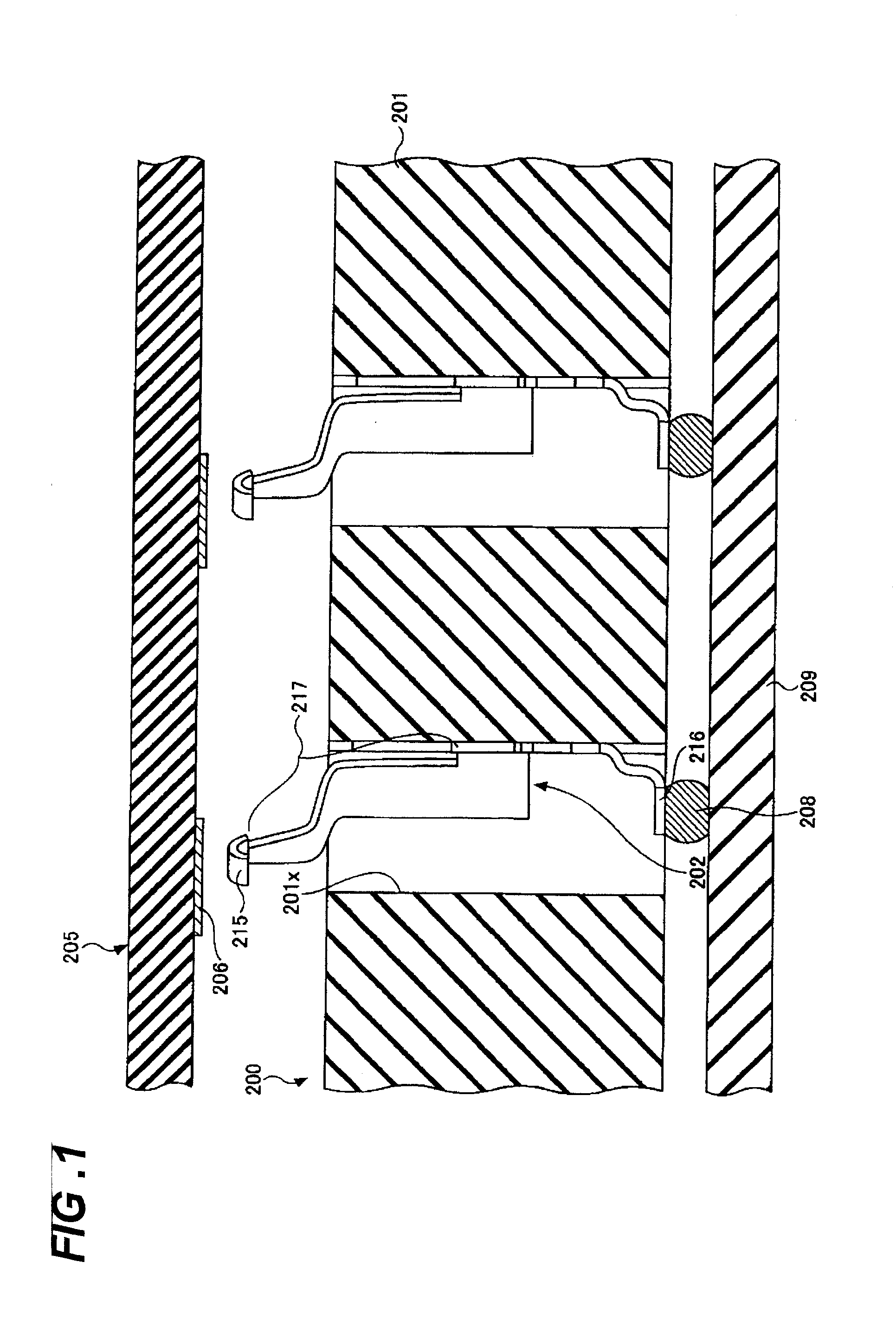
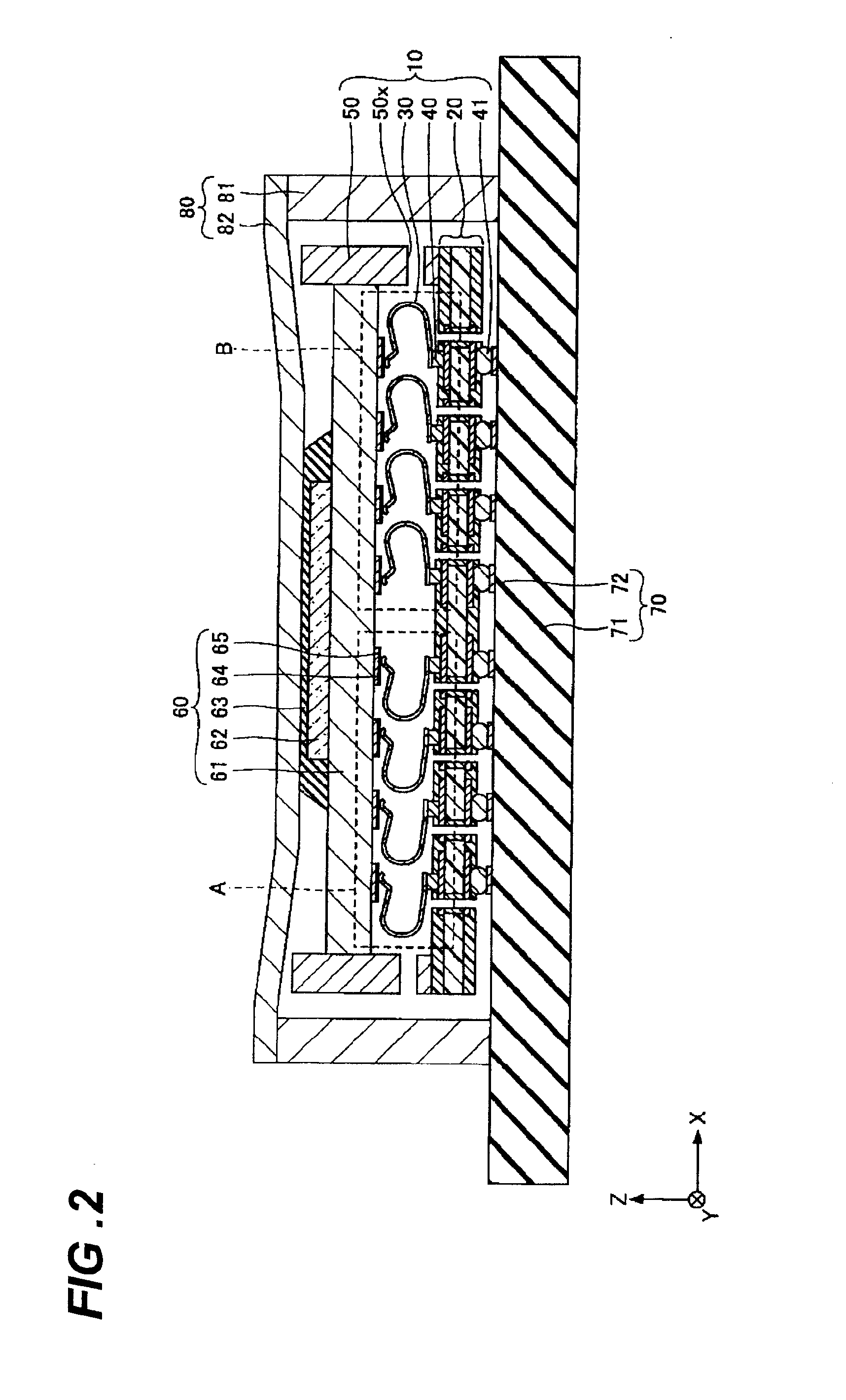
[0044]FIG. 2 is a sectional view of a socket according to the first embodiment. FIG. 3 is an enlarged sectional view of part of FIG. 2. FIG. 4 is a plan view showing an arrangement of connection terminals used the first embodiment. FIG. 5 is a perspective view of a positioning member used in the embodiment. FIGS. 2 and 3 are sectional views taken parallel with the ZX plane. In FIGS. 2-5, the X direction is the arrangement direction of connection terminals 30, the Y direction is the direction that is perpendicular to the X direction and parallel with the a first surface 21a of a substrate body 21, and the Z direction is the direction that is perpendicular to the first surface 21a of the substrate body 21.
[0045]Since as shown in FIG. 4 the connection terminals 30 are inclined from the X direction in a plan view (i.e. when viewed in the Z direction), their sectional shapes cannot be shown in a sectional view taken parallel with the ZX pl...
embodiment 2
[0105]A second embodiment is different from the first embodiment in that the wiring substrate 20 used in the first embodiment is replaced by a substrate 90 which is different in structure than the wiring substrate 20. In the second embodiment, components having the same components in the first embodiment will not be described in detail. In the second embodiment, the height of the side walls of the positioning member 50 and the positions of the holes 50x are different than in the first embodiment and can be determined as appropriate according to the structures of the substrate 90 and the connection terminals 30.
[0106]FIG. 10 is a sectional view of a socket 10A according to the second embodiment. FIG. 11 is an enlarged sectional view of part of FIG. 10. As shown in FIGS. 10 and 11, the socket 10A is different from the socket 10 (see FIGS. 2 and 3) in that the wiring substrate 20 is replaced by the substrate 90.
[0107]The substrate 90 has a substrate body 91 which is formed with through...
embodiment 3
[0117]A third embodiment is different from the first embodiment in that the positioning member 50 is not provided over the wiring substrate 20 and the frame portion of the case is given the function of the positioning member 50 and used for positioning the semiconductor package 60. In the third embodiment, components having the same components in the above-described embodiments will not be described in detail.
[0118]FIG. 12 is a sectional view of a socket 10B according to the third embodiment. As shown in FIG. 12, the socket 10B is different from the socket 10 (see FIGS. 2 and 3) and the socket 10A (see FIGS. 10 and 11) in that the positioning member 50 is not provided over the wiring substrate 20 and a frame portion 83 of a case positions the semiconductor package 60.
[0119]FIGS. 13A, 13B, and 13C are a plan view, a bottom view, and a perspective view, respectively, of the frame portion 83 of the socket 10B according to the third embodiment. As shown in FIGS. 13A-13C, the frame porti...
PUM
 Abstract
Description
Claims
Application Information
 - Generate Ideas
- Intellectual Property
- Life Sciences
- Materials
- Tech Scout
- Unparalleled Data Quality
- Higher Quality Content
- 60% Fewer Hallucinations
Browse by: Latest US Patents, China's latest patents, Technical Efficacy Thesaurus, Application Domain, Technology Topic, Popular Technical Reports.
© 2025 PatSnap. All rights reserved.Legal|Privacy policy|Modern Slavery Act Transparency Statement|Sitemap|About US| Contact US: help@patsnap.com