Optical module and electronic apparatus

a technology of optical modules and electronic devices, applied in the direction of optical radiation measurement, instruments, spectrometry/spectrophotometry/monochromators, etc., can solve the problems of interference filter distortion, interference filter distortion, and deviation in the separated wavelength or half-value width, so as to achieve high spectral accuracy

Active Publication Date: 2012-08-23
SEIKO EPSON CORP
View PDF1 Cites 24 Cited by
  • Summary
  • Abstract
  • Description
  • Claims
  • Application Information

AI Technical Summary

Benefits of technology

[0007]An advantage of some aspects of the invention is to provide an optical module and an electronic apparatus which include an interference filter with high spectral accuracy even in a case where the interference filter is used in an environment having a large temperature change.

Problems solved by technology

However, in a case where the optical module is used in an environment having a large temperature change, stress is generated due to a difference in the thermal expansion coefficients between the transparent substrate, the light receiving element or the like and the interference filter, which causes distortion in the interference filter.
As a result, a problem arises such that the gap between the reflection films becomes uneven, and thus, deviation occurs in the separated wavelength or the half-value width is changed.
In an optical module in the related art, in a case where the optical module is used in an environment having a large temperature change, there is a problem caused by stress generated due to a difference in the thermal expansion coefficients between a fixing portion such as a transparent substrate or a light receiving element and an interference filter.
Further, since a force corresponding to the shear stress is also applied to the interference filter, distortion occurs in the interference filter.
On the other hand, in a case where the Young's modulus of the adhesive layer is larger than 100 kPa, for example, when surrounding temperature is changed, it is difficult to sufficiently suppress the stress generated due to the difference in the thermal expansion coefficients between the fixing portion and the interference filter, which may cause warping in the interference filter.
In a case where a plurality of locations are fixed by the cured adhesive layer, the effect of sufficiently suppressing occurrence of distortion of the interference filter tends to become weak.

Method used


Image

  • Optical module and electronic apparatus
  • Optical module and electronic apparatus
  • Optical module and electronic apparatus

Examples


first embodiment

[0052]Hereinafter, a first embodiment of the invention will be described with reference to the accompanying drawings.

1. Overall Configuration of Optical Device

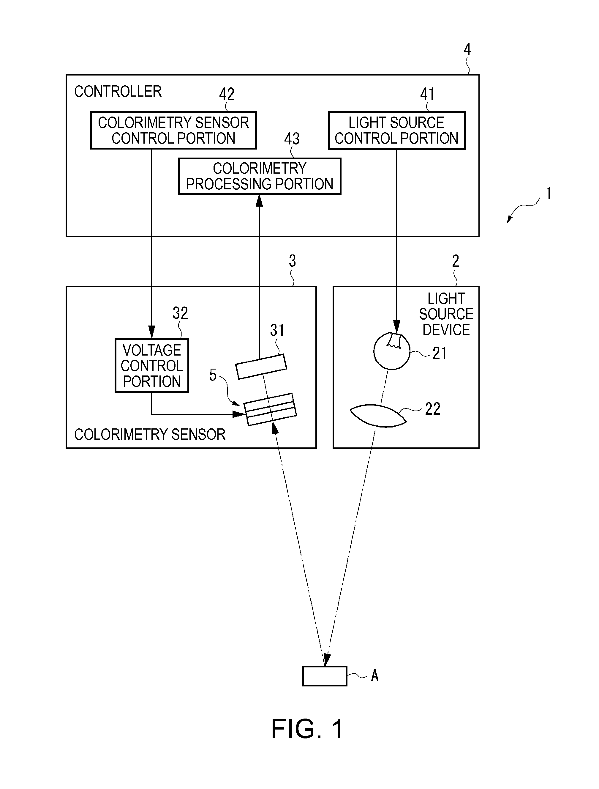
[0053]FIG. 1 is a diagram schematically illustrating a configuration of a colorimeter (electronic apparatus) according to an embodiment of the invention.

[0054]A colorimeter 1 is an electronic apparatus according to the invention, and as shown in FIG. 1, includes alight source device 2 which emits light to a measurement target A, a colorimetry sensor 3 which is an optical module according to the invention, and a controller 4 which controls an overall operation of the colorimeter 1. Further, as the measurement target A reflects light emitted from the light source device 2 and the colorimetry sensor 3 receives the reflected light to be inspected, the colorimeter 1 analyzes and measures the chromaticity of the light to be inspected, that is, the color of the measurement target A on the basis of a detection signal output from the c...

second embodiment

[0097]Next, a second embodiment of the invention will be described with reference to the accompanying drawings.

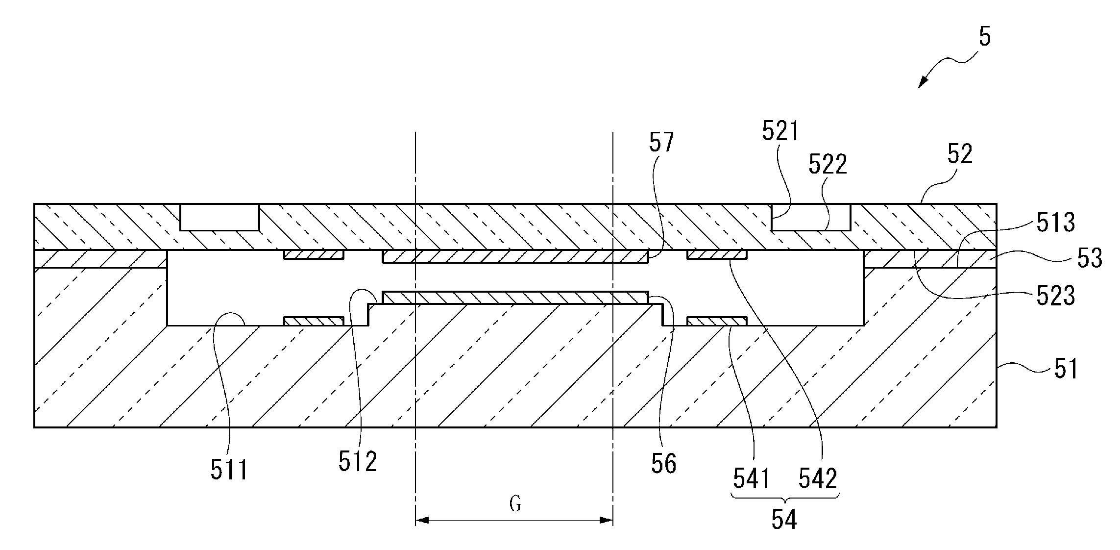
[0098]FIG. 5 is a cross-sectional view illustrating the vicinity of an interference filter 5 in a colorimetry sensor (optical module) according to a second embodiment. Hereinafter, the same reference numerals are given to the same components as in the first embodiment, and its description will be omitted or simplified.

[0099]In the colorimetry sensor 3, as shown in FIG. 5, a part of the interference filter 5 is fixed to the transparent substrate 7 through a cured adhesive layer 61 obtained by curing a curable adhesive agent, and the other part of the interference filter 5 is fixed to the transparent substrate 7 through the adhesive layer 6. Further, the interference filter 5 is connected to the voltage control portion 32 by the wiring R. Further, as shown in FIG. 5, the cured adhesive layer 61 is disposed in a part (one location) of a region which overlaps with a first elect...

third embodiment

[0104]Next, a third embodiment of the invention will be described with reference to the accompanying drawings.

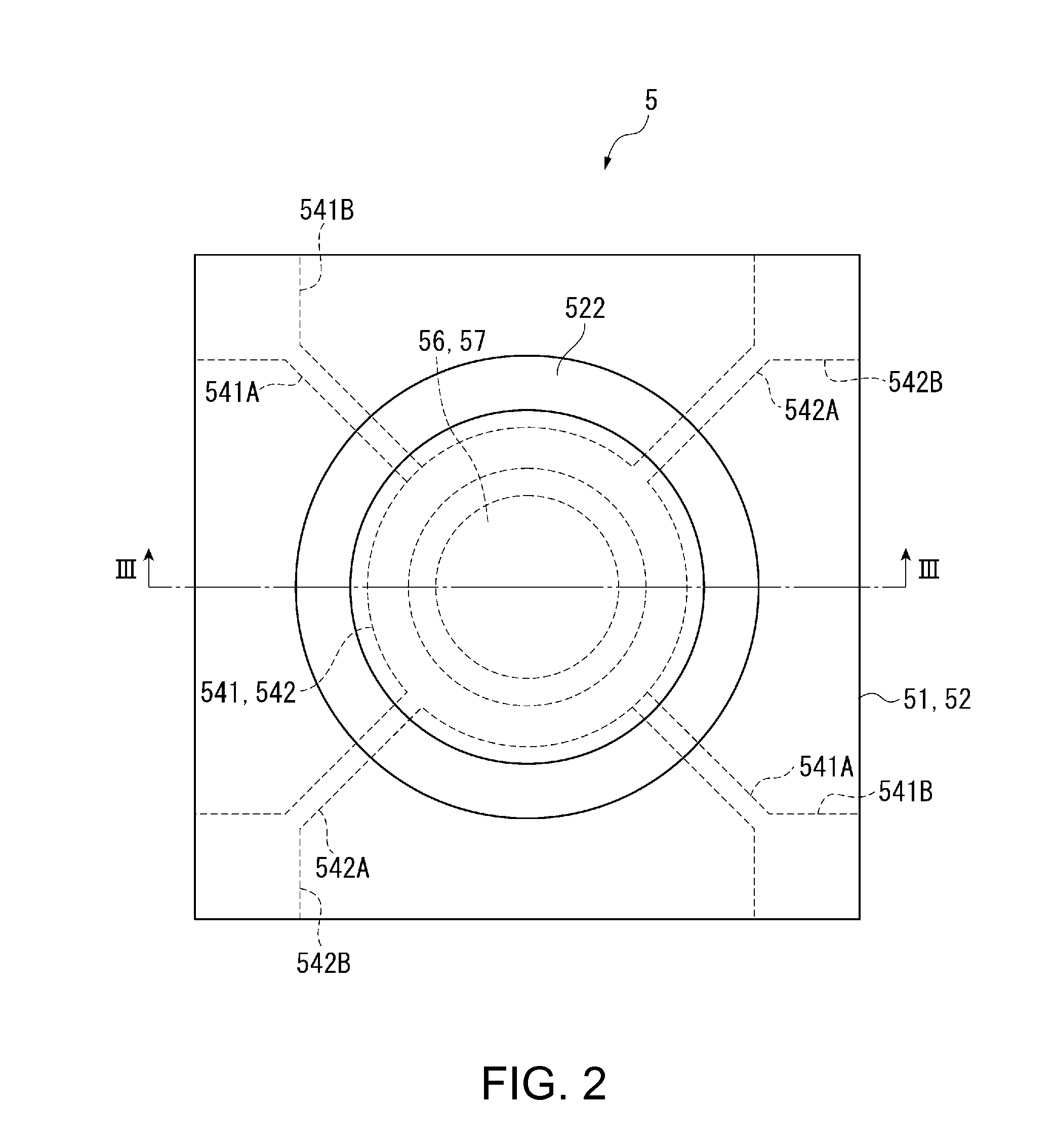
[0105]FIG. 6 is a cross-sectional view illustrating the vicinity of an interference filter 5 in a colorimetry sensor 3 (optical module) according to a third embodiment.

[0106]In the colorimetry sensor 3, as shown in FIG. 6, the interference filter 5 is fixed to the light receiving device 31 through the adhesive layer 6, and the light receiving device 31 is fixed to a support substrate 71 through the cured adhesive layer 61. Further, the interference filter 5 is connected to the voltage control portion 32 by the wiring R. The light receiving device 31 is connected to the colorimetry processing portion 43 by the wiring R. Further, the adhesive layer 6 is disposed in the light transmission region G and a region which overlaps with the light receiving device 31 when seen from a plan view.

[0107]Here, as the support substrate 71, the transparent substrate 7 may be used, but since t...


PUM


Abstract

An optical module (colorimetry sensor) includes an interference filter, and a transparent substrate to which a first substrate of the interference filter is fixed, having a second thermal expansion coefficient which has a value different from a first thermal expansion coefficient. The interference filter is fixed to the transparent substrate through an adhesive layer made of gel-like resin, and the adhesive layer alleviates stress generated due to a difference in the thermal expansion coefficients between the interference filter and the transparent substrate.

Description

BACKGROUND[0001]1. Technical Field[0002]The present invention relates to an optical module and an electronic apparatus which include an interference filter which separates light of a predetermined wavelength from incident light.[0003]2. Related Art[0004]In the related art, an interference filter has been proposed which transmits or reflects only light of a predetermined wavelength from incident light (refer to JP-A-2009-134027, for example).[0005]JP-A-2009-134027 discloses an optical device (interference filter) in which a pair of substrates face each other and reflection films are respectively formed on the surfaces of the substrates which face each other. In such an interference filter, a gap is formed between the pair of reflection films, and the dimension of the gap determines the wavelength of light which can be separated. Thus, in such an interference filter, it is necessary to maintain the pair of reflection films parallel to each other in order to separate light of a predete...

Claims


Application Information

Patent Timeline
Patent Type & Authority Applications(United States)
IPC IPC(8): G02B26/00
CPCG02B5/28G01N21/3504G01J3/50G01J3/51G01J2003/1226G01N21/255G01N21/554G01N21/658G02B26/001G01N21/251
Inventor SAKURAI, KAZUNORI
Owner SEIKO EPSON CORP
Why Eureka
Try Eureka