
Baseline management for input devices

a technology for input devices and baselines, applied in the field of baseline management of input devices, can solve the problems of increasing system cost, increasing system size, and/or needlessly increasing the size of the complete system package, so as to reduce or remove the effect of substantially non-random electrical interference on input, improve the performance of input devices, and reliably and accurately sense the position of input objects

Active Publication Date: 2012-09-13
SYNAPTICS INC
View PDF3 Cites 27 Cited by
  • Summary
  • Abstract
  • Description
  • Claims
  • Application Information

AI Technical Summary

Benefits of technology

[0008]Embodiments of the invention generally provide a method and system that is able to minimize or remove the effect of substantially non-random electrical interference on an input device's ability to reliably and accurately sense the position of an input object. In various embodiments, the substantially non-random electrical interference affects the background capacitance of the sensor device. One or more of the embodiments discussed herein are used to improve the performance of an input device by reducing the affect that the interference has on the position sensing data acquired by the input device.

Problems solved by technology

However, these useful electrical sensing techniques are susceptible to interference, such as electromagnetic interference (EMI), commonly generated by the other supporting components, such as liquid crystal display (LCD) components, that are position near the proximity sensor device.
Current commercial electronic or computing systems have not been able to effectively minimize this type of EMI, and have commonly resorted to finding ways to minimize the magnitude of the interference by distancing the EMI generating components from the proximity sensing device, adding shielding components to the device package, and / or altering the display processing method, thus making the system more expensive and / or needlessly increasing the size of the complete system package.

Method used


Image

  • Baseline management for input devices
  • Baseline management for input devices
  • Baseline management for input devices

Examples


Embodiment Construction

[0029]The following detailed description is merely exemplary in nature and is not intended to limit the invention or the application and uses of the invention. Furthermore, there is no intention to be bound by any expressed or implied theory presented in the preceding technical field, background, brief summary or the following detailed description.

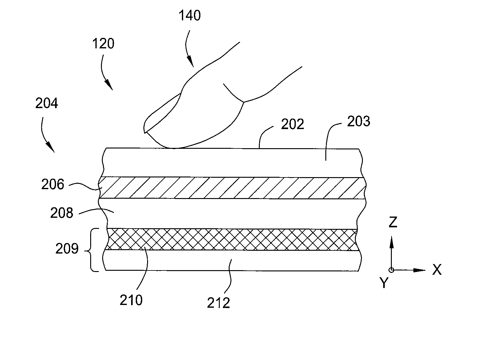
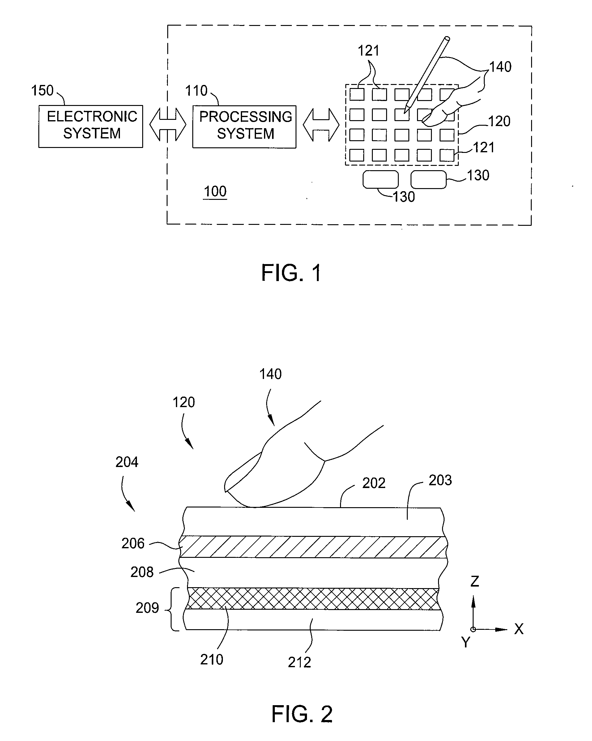
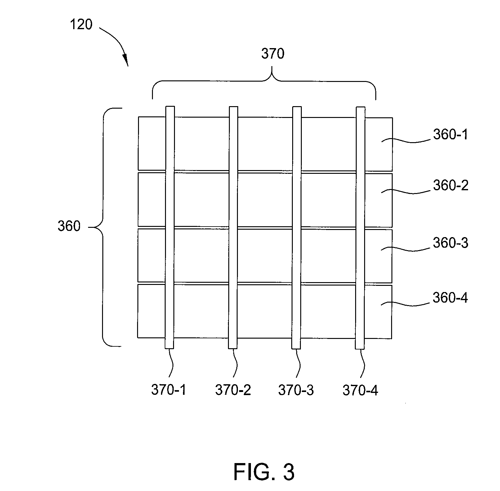
[0030]Embodiments of the invention generally provide a method and system that is able to minimize or remove the effect of substantially non-random electrical interference on an input device's ability to reliably and accurately sense the position of an input object. One or more of the embodiments discussed herein are used to improve the performance of an input device by reducing the affect that the interference has on the position sensing data acquired by the input device. In one embodiment, the input device is configured to systematically correct for a cyclic variation in the electromagnetic interference (EMI) generated by components withi...


PUM


Abstract

Embodiments of the invention generally provide a method and system that is able to minimize or remove the affect of substantially non-random electrical interference on an input device's ability to reliably and accurately sense the position of an object. In one embodiment, the input device is configured to systematically correct for a cyclic variation in the electromagnetic interference (EMI) generated by components within the electronic system, such as interference generated by the process of refreshing or updating an image on a display module that affects the capacitive sensing measurements acquired from a plurality of capacitive sensing elements. However, in some embodiments of the invention, the performance of an input device is improved by reducing the affect that external interference generated outside of the electronic system have on the position sensing data acquired by the input device.

Description

CROSS-REFERENCE TO RELATED APPLICATIONS[0001]This application claims benefit of U.S. Provisional Patent Application Ser. No. 61 / 450,504, filed Mar. 8, 2011, which is herein incorporated by reference.BACKGROUND OF THE INVENTION[0002]1. Field of the Invention[0003]Embodiments of the present invention generally relate to a system and method of sensing an input object's position over a sensing region of a proximity sensing device.[0004]2. Description of the Related Art[0005]Input devices including proximity sensor devices, also commonly called touchpads or touch sensor devices, are widely used in a variety of electronic systems. A proximity sensor device typically includes a sensing region, often demarked by a surface, in which the proximity sensor device determines the presence, location and / or motion of one or more input objects. Proximity sensor devices may be used to provide interfaces for the electronic system. For example, proximity sensor devices are often used as input devices f...

Claims


Application Information

Patent Timeline
IPC IPC(8): G06F3/044
CPCG06F3/044G06F3/0418G06F3/0443G06F3/0445
Inventor SCHWARTZ, ADAMREYNOLDS, JOSEPH KURTHJORDAN, JOEL C.
Owner SYNAPTICS INC
Learn More