Semiconductor devices having nanochannels confined by nanometer-spaced electrodes

Inactive Publication Date: 2012-10-11
IBM CORP
View PDF4 Cites 16 Cited by
  • Summary
  • Abstract
  • Description
  • Claims
  • Application Information

AI Technical Summary

Benefits of technology

[0004]Aspects of the invention include semiconductor devices having integrated nanochannels confined by nanometer spaced electrodes. The semiconductor devices are fabricated using planar, VLSI-based high

Problems solved by technology

A key issue with these techniques is to fabricate nanopores/nanochannels and to integrate electrodes within the nanopore build while enabling electric measurements inside the nanopores/nanochannels.
Due to the sub-10 nm cross-section dimensions of t

Method used


Image

  • Semiconductor devices having nanochannels confined by nanometer-spaced electrodes
  • Semiconductor devices having nanochannels confined by nanometer-spaced electrodes
  • Semiconductor devices having nanochannels confined by nanometer-spaced electrodes

Examples


Embodiment Construction

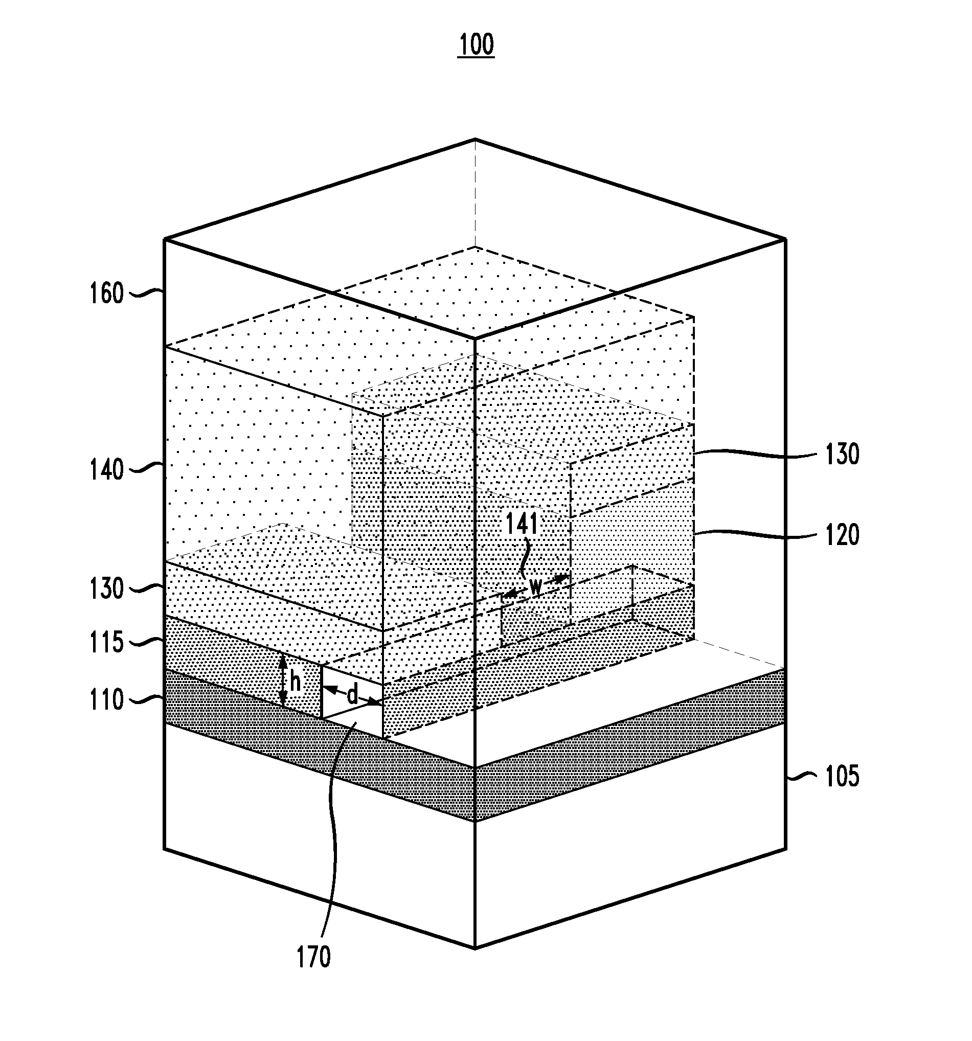
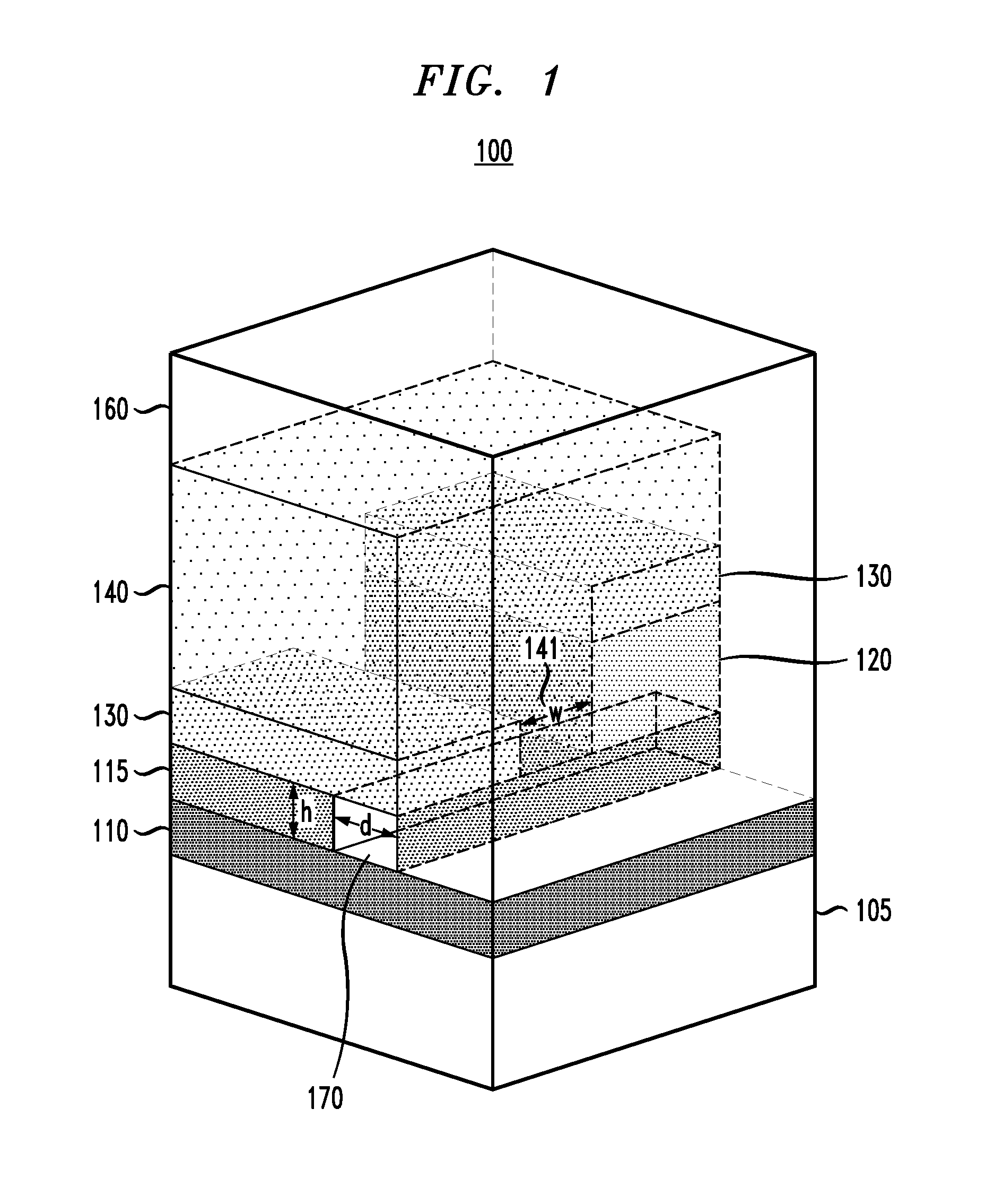
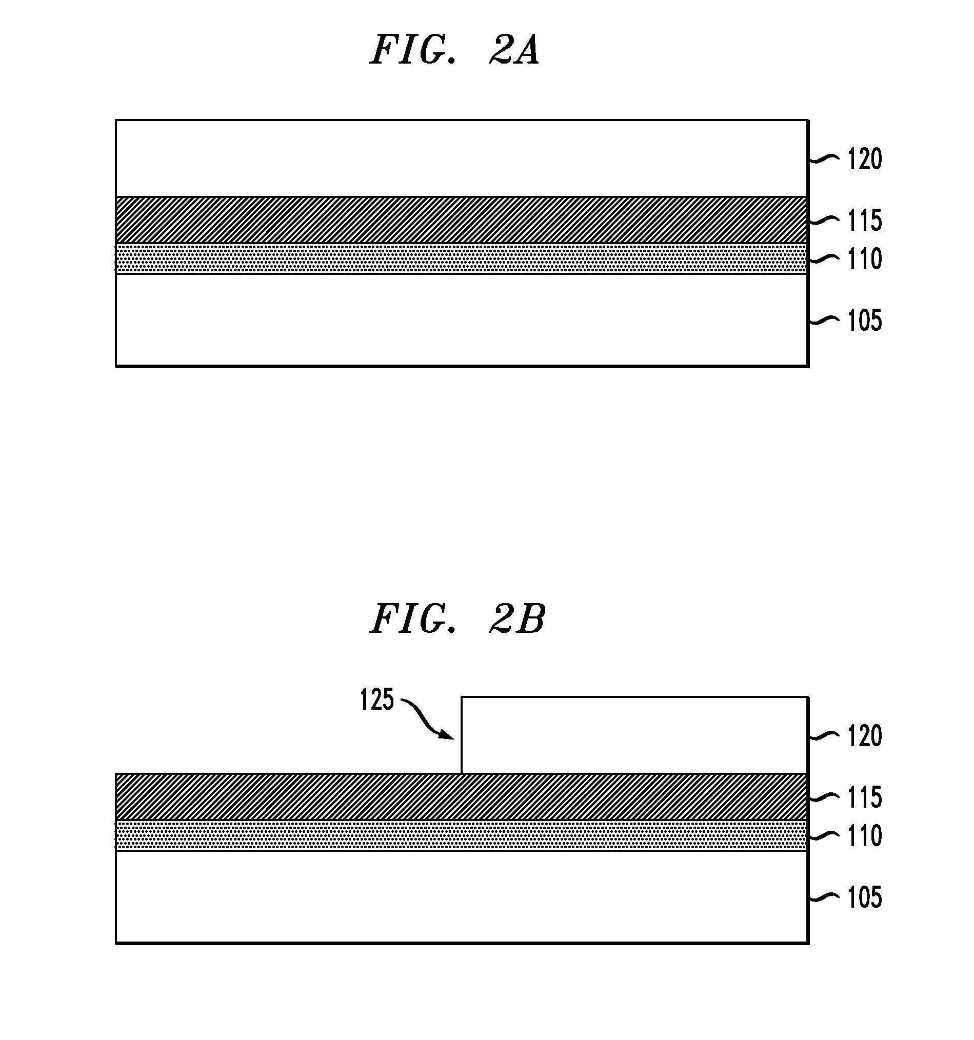
[0027]Preferred embodiments of the invention will now be described in further detail with reference to semiconductor devices having integrated nanochannels confined by nanometer spaced electrodes, and VLSI (very large scale integration) planar fabrication methods for constructing semiconductor devices having integrated nanochannels confined by nanometer spaced electrodes. It is to be understood that the invention is not limited to the particular materials, features, and processing steps shown and described herein. Modifications to the illustrative embodiments will become apparent to those of ordinary skill in the art. It should also be understood that the various layers and / or regions shown in the accompanying figures are not drawn to scale, and that one or more semiconductor layers and / or regions of a type commonly used in such integrated circuits may not be explicitly shown in a given figure for ease of explanation. Particularly with respect to processing steps, it is to be emphas...


PUM

PropertyMeasurementUnit
Widthaaaaaaaaaa
Widthaaaaaaaaaa
Surface areaaaaaaaaaaa

Abstract

Semiconductor devices having integrated nanochannels confined by nanometer spaced electrodes, and VLSI (very large scale integration) planar fabrication methods for making the devices. A semiconductor device includes a bulk substrate and a first metal layer formed on the bulk substrate, wherein the first metal layer comprises a first electrode. A nanochannel is formed over the first metal layer, and extends in a longitudinal direction in parallel with a plane of the bulk substrate. A second metal layer is formed over the nanochannel, wherein the second metal layer comprises a second electrode. A top wall of the nanochannel is defined at least in part by a surface of the second electrode and a bottom wall of the nanochannel is defined by a surface of the first electrode.

Description

CROSS-REFERENCE TO RELATED APPLICATION[0001]This application claims priority to U.S. Provisional Patent Application Ser. No. 61 / 472,349, filed on Apr. 6, 2011, the disclosure of which is fully incorporated herein by reference.TECHNICAL FIELD[0002]This invention relates generally to semiconductor devices having integrated nanochannels confined by nanometer spaced electrodes, and VLSI (very large scale integration) planar fabrication methods for constructing semiconductor devices having integrated nanochannels confined by nanometer spaced electrodes.BACKGROUND[0003]Recently, there has been growing interest in utilizing nanopores / nanochannels as sensors for rapid analysis of biomolecules such as DNA, RNA, protein, etc. Special emphasis has been given to applications of nanopores / nanochannels for DNA sequencing, as this technology will enable reductions in the cost of sequencing below $1000 / human genome. A key issue with these techniques is to fabricate nanopores / nanochannels and to int...

Claims


Application Information

Patent Timeline
IPC IPC(8): H01L29/66H01L21/283B82Y99/00
CPCB82Y40/00Y10S977/958H01L21/82B82Y15/00
Inventor HARRER, STEFANPOLONSKY, STANISLAVKETCHEN, MARK B.OTT, JOHN A.
Owner IBM CORP
Why Eureka
Try Eureka