

Light-emitting diode in semiconductor material
a technology of light-emitting diodes and semiconductor materials, which is applied in the direction of solid-state devices, basic electric elements, electric devices, etc., can solve the problems of weak exciton energy, limiting the production of leds from zno, and weak acceptor concentration and hole mobility
- Summary
- Abstract
- Description
- Claims
- Application Information
AI Technical Summary
Benefits of technology
Problems solved by technology
Method used
Image

Examples
Embodiment Construction
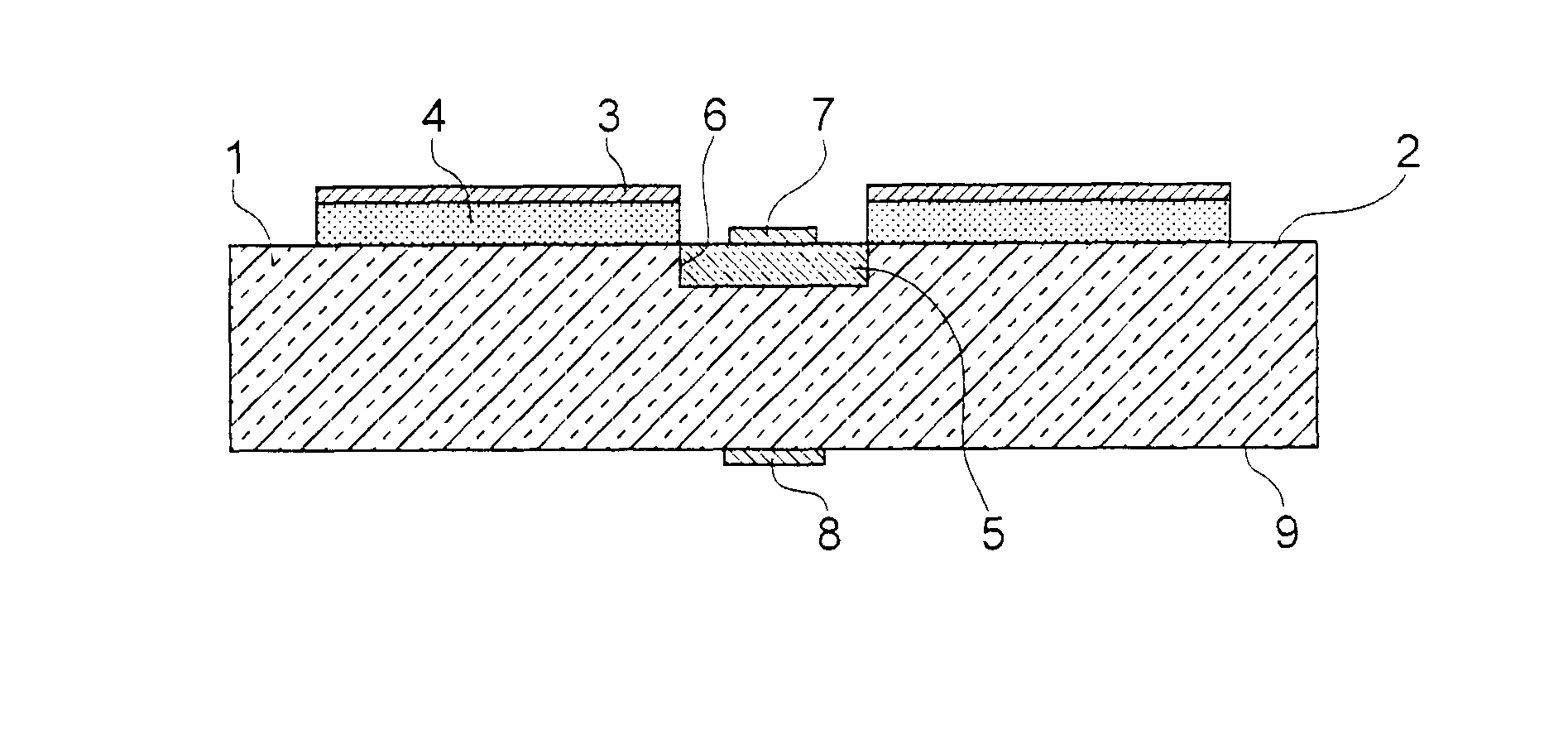
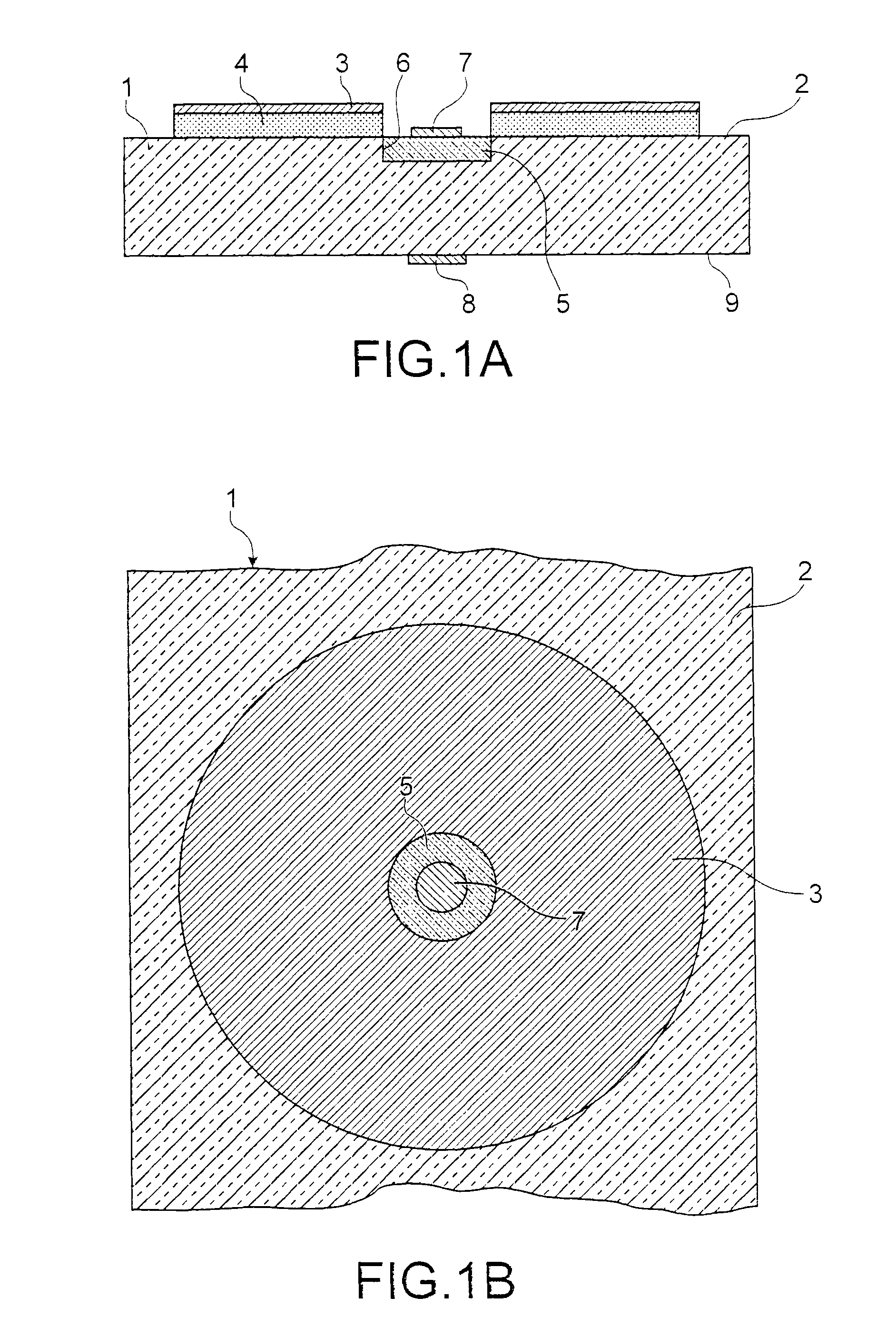
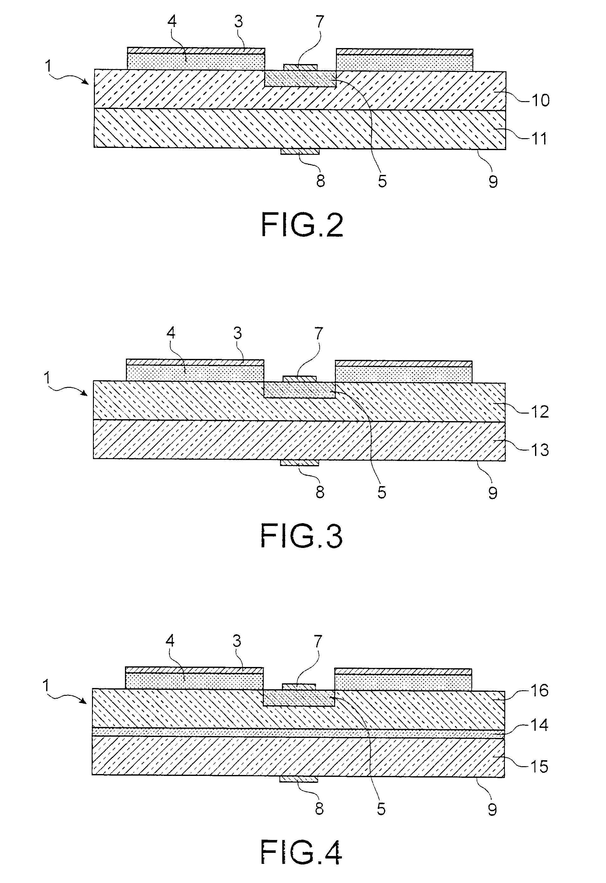
[0011]The present invention is designed to allow by-passing of the problem related to ZnO p-doping, by inverting dope type in a region of a ZnO structure using a gate. This technique can be applied to any semiconductor material to cause light emission, in particular to materials such as ZnO, GaN, GaAs. It can be used to fabricate LED matrices of micrometric size that are easily addressable, for display purposes for example, each LED of the matrix forming a picture element or pixel.
[0012]One first subject of the invention is a light-emitting diode comprising a structure in semiconductor material having a first conductivity type, and means for electric polarisation of the diode, characterized in that:[0013]the structure has a first face of which a first region is in contact with a pad in semiconductor material having a second type of conductivity opposite the first conductivity type,[0014]the polarising means comprise:[0015]an electric contact on the pad,[0016]an electric contact on t...
PUM
 Abstract
Description
Claims
Application Information