
Method for making semi-conductor nanocrystals oriented along a predefined direction

Inactive Publication Date: 2012-11-08
COMMISSARIAT A LENERGIE ATOMIQUE ET AUX ENERGIES ALTERNATIVES +1
View PDF7 Cites 1 Cited by
  • Summary
  • Abstract
  • Description
  • Claims
  • Application Information

AI Technical Summary

Problems solved by technology

To be unable to choose the orientation of the elongated shape semi-conductor nanocrystals can raise problems, for example when the nanocrystals are to be part of electronic nanodevices and that these nanocrystals are to be at a controlled distance from other elements such as electrodes of nanodevices.

Method used


Image

  • Method for making semi-conductor nanocrystals oriented along a predefined direction
  • Method for making semi-conductor nanocrystals oriented along a predefined direction
  • Method for making semi-conductor nanocrystals oriented along a predefined direction

Examples


Embodiment Construction

[0008]Thus there is a need to provide a method for making semi-conductor nanocrystals enabling not only the dimensions and density of the semi-conductor nanocrystals, but also the orientation of semi-conductor nanocrystals made by dewetting of the semi-conductor, to be controlled regardless the nature (amorphous or crystalline) of the material underlying the semi-conductor.

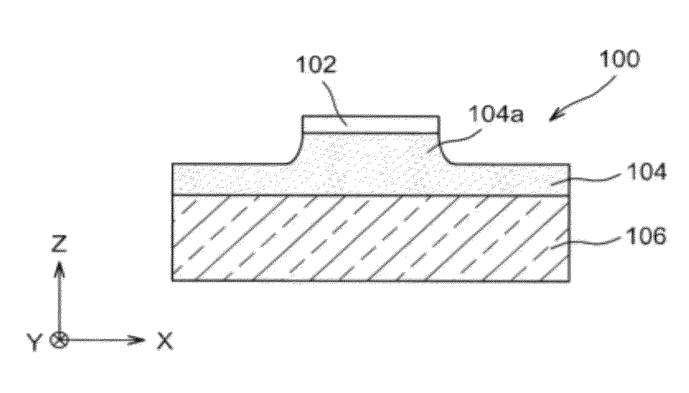
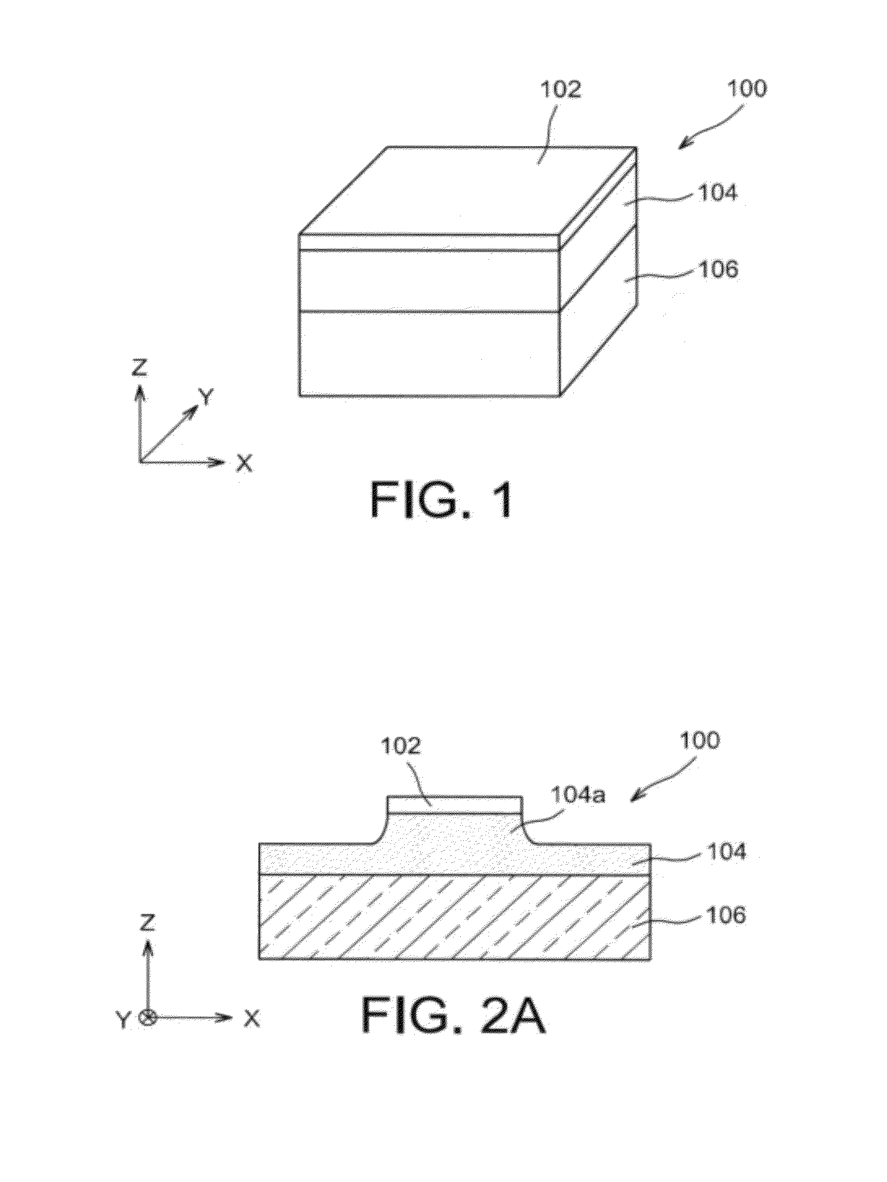
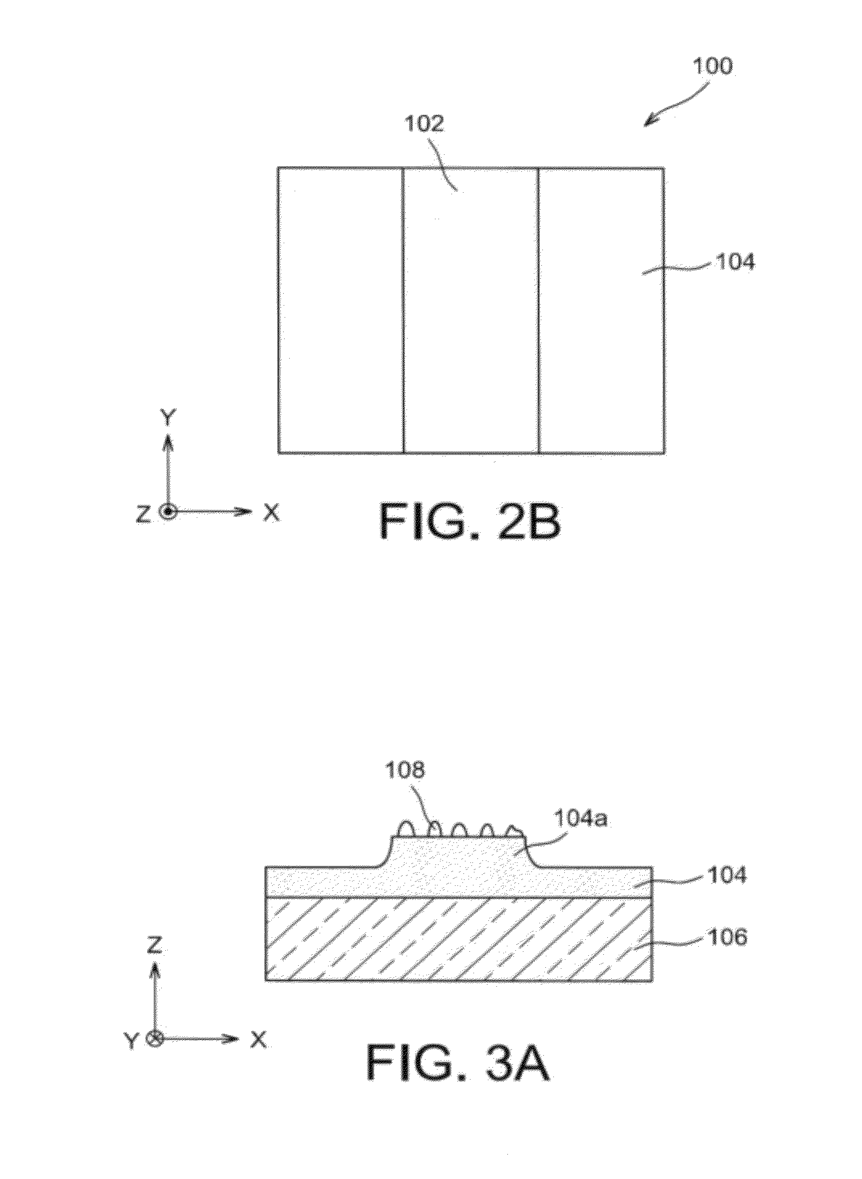
[0009]To do this, one embodiment provides a method for making semi-conductor nanocrystals, including at least the steps of:[0010]making a stack of at least one uniaxially stressed semi-conductor thin layer and a dielectric layer,[0011]annealing the semi-conductor thin layer such that a dewetting of the semi-conductor forms, on the dielectric layer, elongated shaped semi-conductor nanocrystals oriented perpendicularly to the stress axis.

[0012]Because the uniaxial stress is exerted on the semi-conductor thin layer, the dewetting of the semi-conductor results in semi-conductor nanocrystals in view of the elastic stre...


PUM


Abstract

A method for making a semi-conductor nanocrystals, including at least the steps of:making a stack of at least one uniaxially stressed semi-conductor thin layer and a dielectric layer,annealing the semi-conductor thin layer such that a dewetting of the semi-conductor forms, on the dielectric layer, elongated shaped semi-conductor nanocrystals oriented perpendicularly to the stress axis.

Description

TECHNICAL FIELD[0001]The invention relates to a method for making semi-conductor nanocrystals obtained by dewetting a thin layer of this semi-conductor provided on a dielectric layer, oriented along a direction selected beforehand and which can be used for making microelectronic and / or nanoelectronic devices, for example memory devices.[0002]The invention also relates to a method for making a porous dielectric layer resorting to semi-conductor nanocrystals oriented along a predefined direction.STATE OF PRIOR ART[0003]For making semi-conductor nanocrystals, that is semi-conductor aggregates the dimensions of which can be between about a few nanometres and a few hundred nanometres, it is known to make a dewetting of a silicon thin layer provided on a SiO2 layer. Indeed, when the silicon thin layer, corresponding for example to the active layer, or upper layer, of a SOI (silicon on insulator) substrate, is subjected to a high temperature (for example between about 650° C. and 1250° C.)...

Claims


Application Information

Patent Timeline
IPC IPC(8): H01L21/20B82Y40/00
CPCB82Y10/00B82Y40/00H01L21/02381H01L21/02488H01L21/02529B82Y30/00H01L21/02538H01L21/0259H01L21/02667H01L29/0665H01L29/127H01L21/02532
Inventor BOROWIK, LUKASZBARBE, JEAN-CHARLESBUSSMANN, EZRACHEYNIS, FABIENLEROY, FREDERICMARIOLLE, DENISMULLER, PIERRE
Owner COMMISSARIAT A LENERGIE ATOMIQUE ET AUX ENERGIES ALTERNATIVES
Learn More