Semiconductor light-emitting structure

Active Publication Date: 2012-11-22
EPISTAR CORP
View PDF4 Cites 2 Cited by
  • Summary
  • Abstract
  • Description
  • Claims
  • Application Information

AI Technical Summary

Benefits of technology

[0008]Accordingly, the invention is directed to a semiconductor light-emitting structure capable of effectively advancing the uniformity of the exiting light.
[0011]In the semiconductor light-emitting structure of the embodiments of the invention, the first electrical transmission layer connected to the first conductors serves as an extension of the first conductors, so that the semiconductor light-emitting structure of the embodiments of the invention can make the current more dispersed. In this way, the semiconductor light-emitting structure of the embodiments of the invention can effectively resolve the problem of non-uniform current distribution and thereby advance the light exiting efficiency.

Problems solved by technology

When the distribution area of the two electrodes is small, the situation that the light emitted from the light-emitting layer is blocked by the two electrodes can be reduced and the light extraction rate can be accordingly not decreased, however, the current flowing from the p-type semiconductor layer to the n-type semiconductor layer would be excessively concentrated in a small area between the two electrodes.
As a result of excessively concentrated current distribution, it leads to non-uniformity of the emitted light and to heat-dissipation difficulty and easier damage of the LED due to the excessively concentrated heat produced during the current passing, and the LED's light-emitting efficiency is reduced.
On the other hand, when the distribution range between the two electrodes is increased by design, the excessively concentrated current distribution problem can be lightened, but the electrodes would block too much light, which leads to largely reducing the light extraction rate.

Method used


Image

  • Semiconductor light-emitting structure
  • Semiconductor light-emitting structure
  • Semiconductor light-emitting structure

Examples


Embodiment Construction

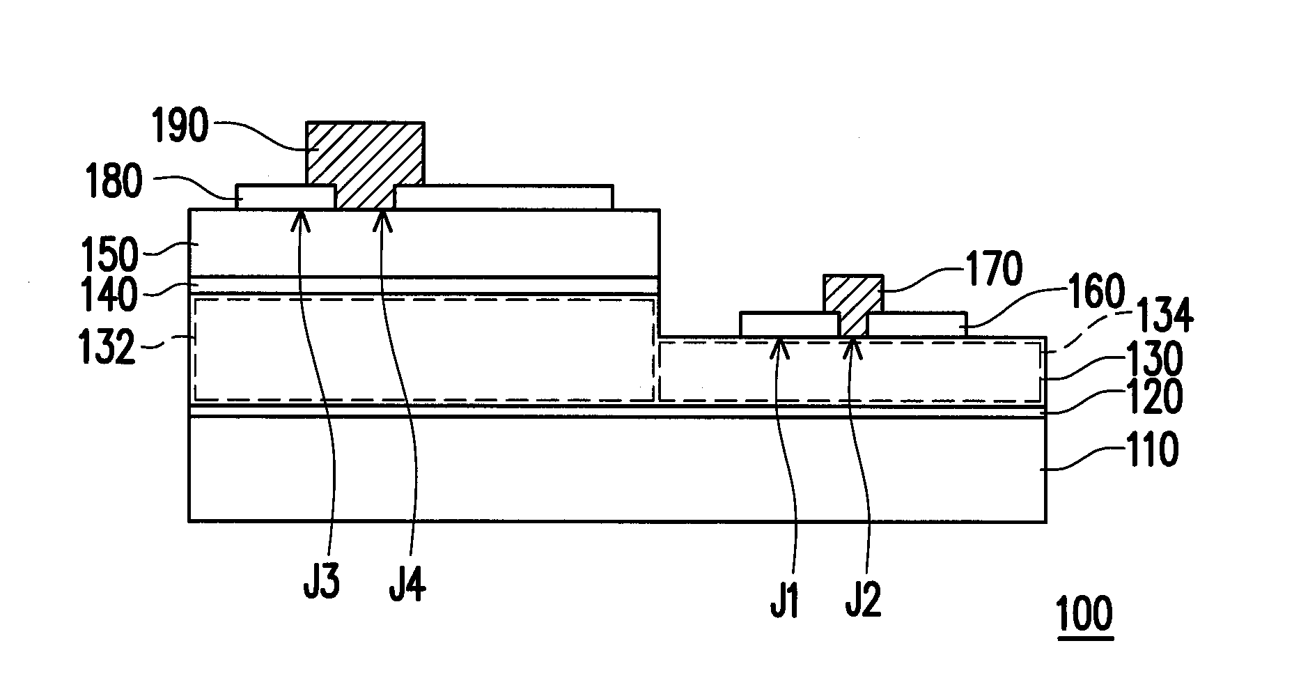
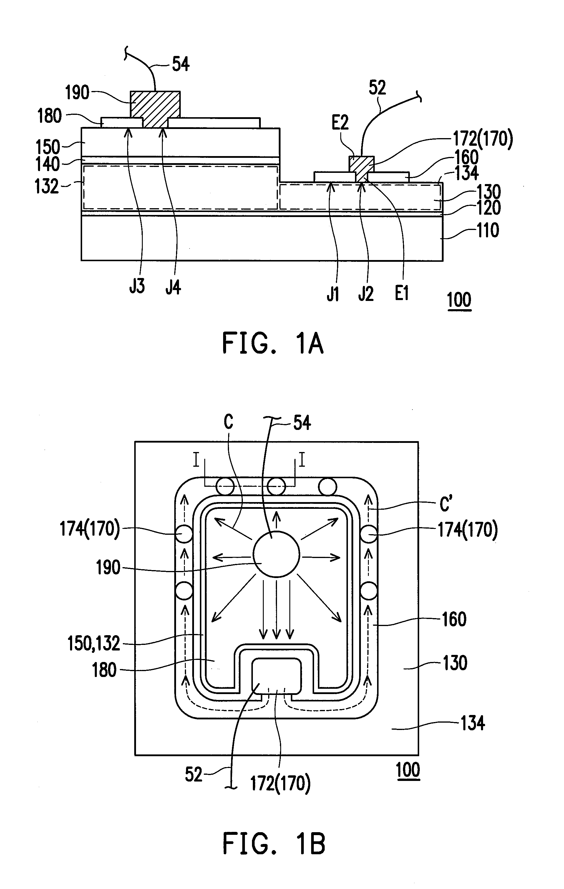
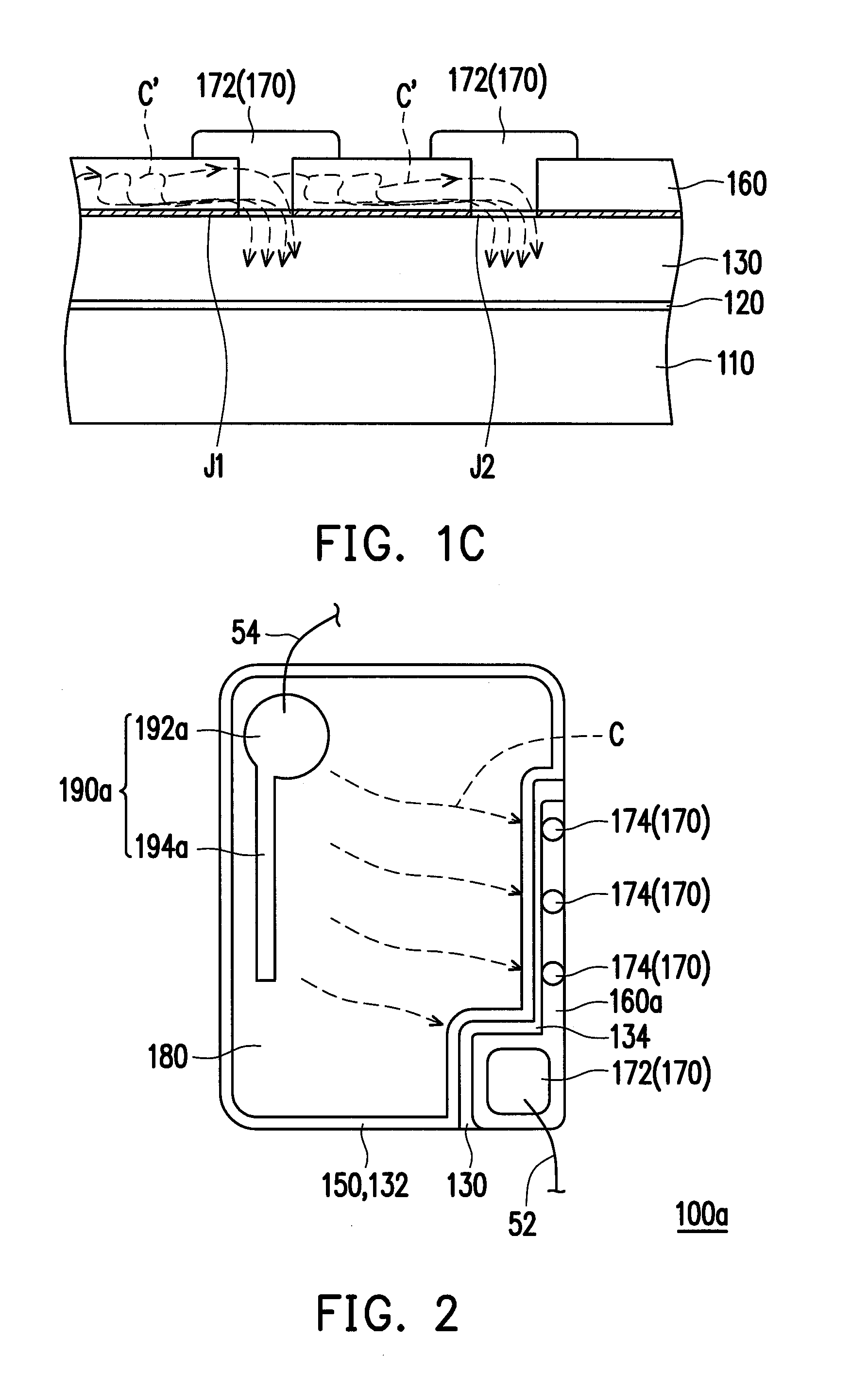
[0020]FIG. 1A is a cross-sectional schematic diagram of a semiconductor light-emitting structure according to an embodiment of the invention, FIG. 1B is a top-view schematic diagram of the semiconductor light-emitting structure of FIG. 1A and FIG. 1C is a localized cross-sectional schematic diagram of the semiconductor light-emitting structure of FIG. 1B along line I-I. Referring to FIGS. 1A-1C, a semiconductor light-emitting structure 100 of the embodiment is, for example, an LED die structure and includes a first doped type semiconductor layer 130, a light-emitting layer 140, a second doped type semiconductor layer 150, a first electrical transmission layer 160 and at least a first conductor 170 (in the embodiment, it is a plurality of first conductors 170 as an example). The light-emitting layer 140 is disposed over the first doped type semiconductor layer 130 and the second doped type semiconductor layer 150 is disposed over the light-emitting layer 140. In the embodiment, the f...


PUM


Abstract

A semiconductor light-emitting structure is provided, which includes a first doped type semiconductor layer, a light-emitting layer, a second doped type semiconductor layer, a first electrical transmission layer and at least one first conductor. The light-emitting layer is disposed on the first doped type semiconductor layer and the second doped type semiconductor layer is disposed on the light-emitting layer. The first electrical transmission layer is disposed on the first doped type semiconductor layer, in which a first interface is formed between the first electrical transmission layer and the first doped type semiconductor layer. The first conductor is disposed on the first doped type semiconductor layer. The first electrical transmission layer connects the first conductor. A second interface is formed between each of the first conductor and the first doped type semiconductor layer, and the resistance of the second interface is less than the resistance of the first interface.

Description

CROSS-REFERENCE TO RELATED APPLICATION[0001]This application claims the priority benefit of Taiwan application serial no. 100117781, filed on May 20, 2011. The entirety of the above-mentioned patent application is hereby incorporated by reference herein and made a part of this specification.BACKGROUND OF THE INVENTION[0002]1. Field of the Invention[0003]The invention generally relates to a light-emitting structure, and more particularly, to a semiconductor light-emitting structure.[0004]2. Description of Related Art[0005]Along with the progress of photoelectric technology, the fabrication and the application of a light-emitting diode (LED) has gradually reached their ripe stage. Since[0006]LEDs have advantages of low pollution, low power consumption, short response time and long lifetime, so that LEDs have been gradually applied in various fields of light source or illumination to substitute traditional light-emitting components such as fluorescent lamp, incandescent bulb or halogen...

Claims


Application Information

Patent Timeline
IPC IPC(8): H01L33/02
CPCH01L33/20H01L33/40H01L33/38H01L2224/49107H01L2224/0603
Inventor LI, JUN-SHENGWU, KUO-CHENWEN, WEI-CHIH
Owner EPISTAR CORP
Why Eureka
Try Eureka