Semiconductor light emitting device and method of manufacturing the same

a technology of semiconductors and light emitting devices, which is applied in the manufacture of semiconductor/solid-state devices, semiconductor devices, and semiconductor devices, etc., can solve the problems of reducing the efficiency of light extraction, and achieve the effect of superior light reflectance and heat dissipation characteristics

Active Publication Date: 2012-11-29
SAMSUNG ELECTRONICS CO LTD
View PDF3 Cites 14 Cited by
  • Summary
  • Abstract
  • Description
  • Claims
  • Application Information

AI Technical Summary

Benefits of technology

[0008]An aspect of the present invention provides a semiconductor light emitting device including a reflector structure on a rear surface of a growth substrate, the reflector structure having superior light reflectance and heat dissipation characteristics.

Problems solved by technology

As a result, a considerable amount of light generated from an active layer is totally internally reflected to be emitted in a substantially undesired direction or be lost in a total internal reflection process, whereby light extraction efficiency may be reduced.

Method used


Image

  • Semiconductor light emitting device and method of manufacturing the same
  • Semiconductor light emitting device and method of manufacturing the same
  • Semiconductor light emitting device and method of manufacturing the same

Examples


Embodiment Construction

[0036]Embodiments of the present invention will now be described in detail with reference to the accompanying drawings.

[0037]The invention may, however, be embodied in many different forms and should not be construed as being limited to the embodiments set forth herein. Rather, these embodiments are provided so that this disclosure will be thorough and complete, and will fully convey the scope of the invention to those skilled in the art.

[0038]In the drawings, the shapes and dimensions of elements maybe exaggerated for clarity, and the same reference numerals will be used throughout to designate the same or like elements.

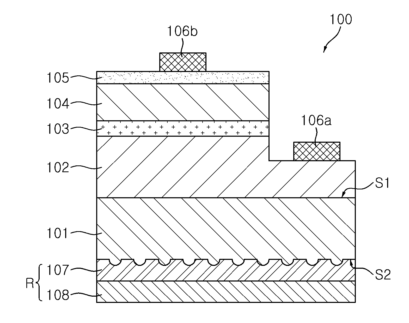
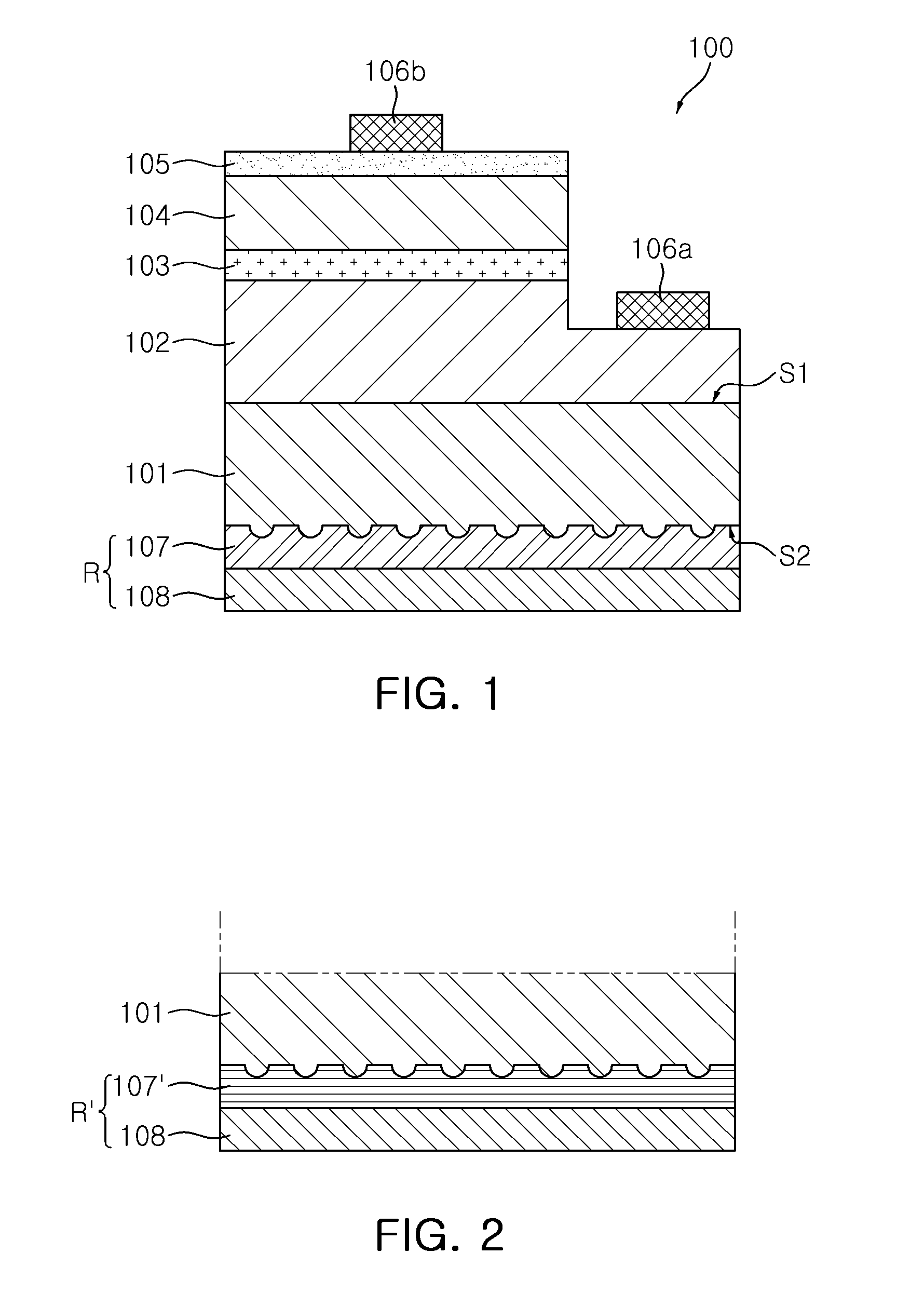
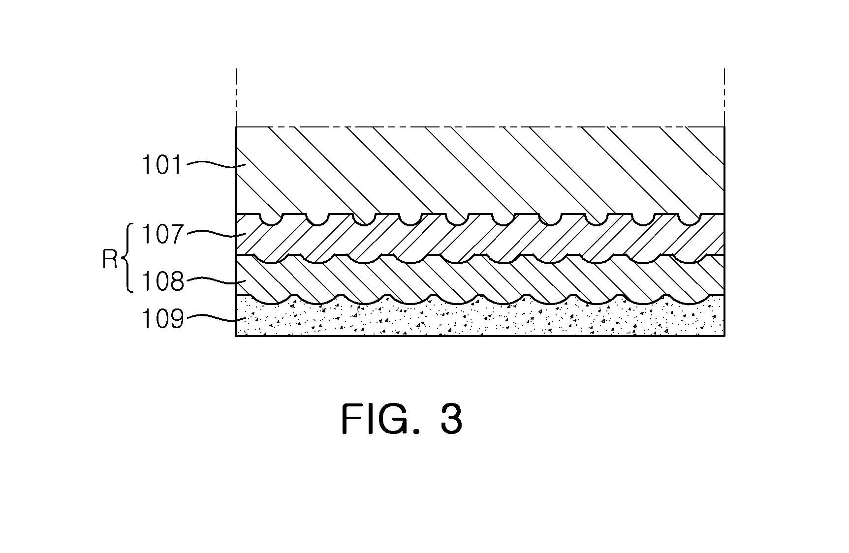
[0039]FIG. 1 is a schematic cross-sectional view illustrating a semiconductor light emitting device according to an embodiment of the invention. FIGS. 2 and 3 are schematic cross-sectional views illustrating the structure of a rear reflective part according to a modification of the embodiment of FIG. 1. With reference to FIG. 1, a semiconductor light emitting device...


PUM


Abstract

There is provided a semiconductor light emitting device including: a light transmissive substrate; a light emitting part; first and second electrodes electrically connected to the first and second conductivity type semiconductor layers, respectively; and a rear reflective part including a reflective metallic layer, and a light transmissive dielectric layer interposed between the light transmissive substrate and the reflective metallic layer.

Description

CROSS-REFERENCE TO RELATED APPLICATIONS[0001]This application claims the priority of Korean Patent Application No. 10-2011-0048368 filed on May 23, 2011, in the Korean Intellectual Property Office, the disclosure of which is incorporated herein by reference.BACKGROUND OF THE INVENTION[0002]1. Field of the Invention[0003]The present invention relates to a semiconductor light emitting device and a method of manufacturing the same.[0004]2. Description of the Related Art[0005]A light emitting diode (LED) is a semiconductor device able to emit light of various colors due to electron-hole recombination occurring at a p-n junction between p-type and n-type semiconductors when current is applied thereto. Such an LED is advantageous over a filament-based light emitting device in that it has a long lifespan, low power consumption, superior initial-operation characteristics, and the like. These factors have continually boosted the demand for LEDs. Notably of late, a great deal of attention has...

Claims


Application Information

Patent Timeline
Patent Type & Authority Applications(United States)
IPC IPC(8): H01L33/60H01L33/62
CPCH01L33/46H01L33/20H01L2224/32225H01L2224/48091H01L2224/48227H01L2224/49107H01L2224/73265H01L2224/83385
Inventor KIM, TAE HUNCHAE, SEUNG WANKIM, YONG ILLEE, SEUNG JAEJANG, TAE SUNGSOHN, JONG RAKKIM, BO KYOUNG
Owner SAMSUNG ELECTRONICS CO LTD
Why Eureka
Try Eureka