Chip component, substrate and electronic apparatus

Inactive Publication Date: 2013-01-03
SONY MOBILE COMM INC
View PDF2 Cites 1 Cited by
  • Summary
  • Abstract
  • Description
  • Claims
  • Application Information

AI Technical Summary

Benefits of technology

[0011]The above-described configuration allows for adjusting the constant or the like of a chip component without changing the internal configuration of the chip component or replacing the chip component.
[0012]Further, the adjustment of the consta

Problems solved by technology

The constant, impedance, etc. of the above-described chip component is reliably determined for each chip component, and it is difficult to adjust the value once a choice is made.
However, since the environment of the surroundings of components that are provided on the surface of the substrate is different from that of the surroundings of components that are provided in the subs

Method used


Image

  • Chip component, substrate and electronic apparatus
  • Chip component, substrate and electronic apparatus
  • Chip component, substrate and electronic apparatus

Examples


Embodiment Construction

[0031]Hereinafter, preferred embodiments will be described in detail with reference to drawings.

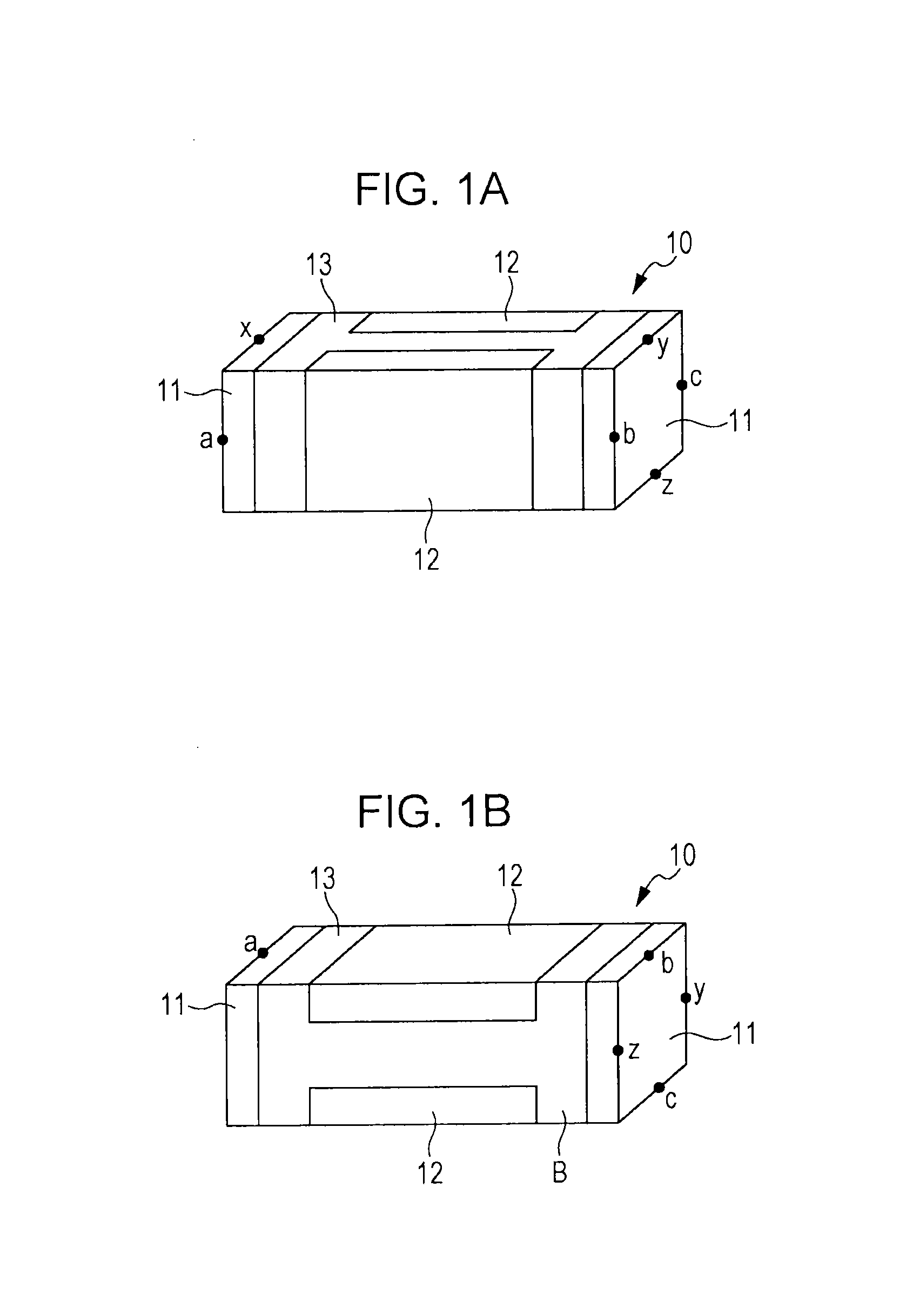
[0032]First, exemplary external views of a chip component (also simply referred to as a chip) having a typical configuration according to the present embodiment are shown in FIGS. 1(a) and 1(b). FIG. 1(a) and FIG. 1(b) are external views of the same chip component viewed from different points.

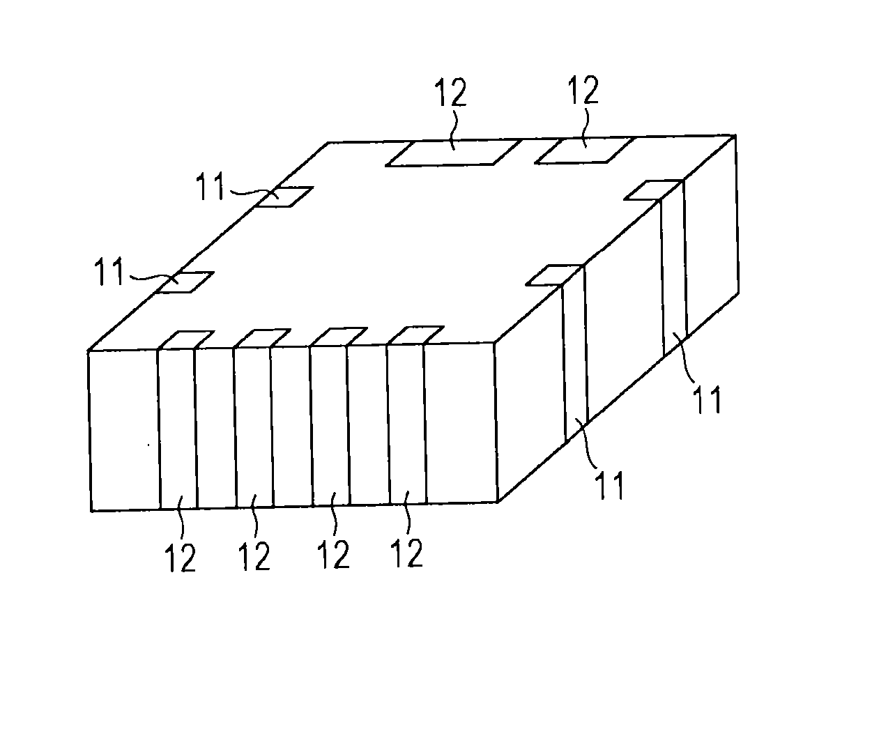
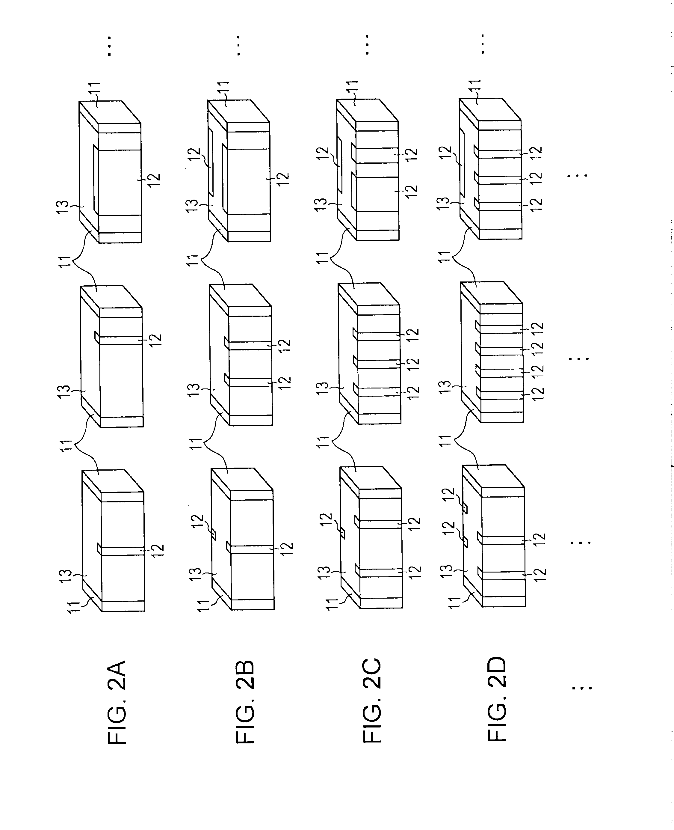
[0033]A chip component 10 includes input and output terminals 11 which are first and second terminals that are provided on the surfaces of both end parts of a dielectric block (substrate) 13 provided as an almost rectangular parallelepiped-shaped dielectric (insulator). The chip component 10 further includes at least one adjustment terminal 12 which is a third terminal provided on the block surface lying between both the end parts. Here, two adjustment terminals 12 are shown.

[0034]For each of the chip components 10, at least one circuit (inter-terminal circuit) connected between at least one set of t...


PUM


Abstract

A chip component is provided with a block including a dielectric, input and output terminals, which are the first and second terminals that are provided on the surface of the block, an adjustment terminal that is a third terminal that includes an internal electrode extended into the block and that is provided on the surface of the block, and at least two inter-terminal circuits that are provided in the block and that are connected between at least two sets of two terminals of the first, second, and third terminals.

Description

CROSS REFERENCE TO RELATED APPLICATION[0001]The present application claims the benefit of the earlier filing date of U.S. provisional application 61 / 503,831 filed on Jul. 1, 2011, the entire contents of which being incorporated herein by reference.TECHNICAL FIELD[0002]The present disclosure relates to a chip component, substrate and electronic apparatus that includes the chip component, and particularly relates to a chip component that can adjust, for example, a constant thereof, and a circuit substrate including the chip component.BACKGROUND ART[0003]Hitherto, a chip component has been appreciated as an electronic component that is directly mounted on the surface of a circuit substrate through surface mounting technology that allows for downsizing an electronic component, increasing the mounting density, etc., in electronic equipment. A solder material is applied to the terminal part of the chip component or a connection part defined on a circuit substrate for mounting in advance, ...

Claims


Application Information

Patent Timeline
IPC IPC(8): H05K7/06H05K7/02H01F21/12H01C10/06H01G4/38
CPCH05K1/029H05K1/185H05K2201/10212H05K2201/10636H01F2017/0026H01G4/38H01G4/40H01C1/16H01G4/228H05K2203/173H01L2224/16227H01L2924/15313H01L2924/3025H01F5/00Y02P70/50
Inventor FUJIMORI, KOTARO
Owner SONY MOBILE COMM INC
Why Eureka
Try Eureka