Liquid crystal display panel and liquid crystal display device

a liquid crystal display panel and display panel technology, applied in the field of liquid crystal display panel and liquid crystal display device, can solve the problems of large deterioration of image quality such as contrast and color tone, unsuitable for applications, and increased risk of image roughness and display unevenness, and achieve high-quality display and wide viewing angle characteristic

Active Publication Date: 2013-02-07
UNIFIED INNOVATIVE TECH
View PDF0 Cites 6 Cited by
  • Summary
  • Abstract
  • Description
  • Claims
  • Application Information

AI Technical Summary

Benefits of technology

[0039]As above described, the liquid crystal display panel of the present invention includes the plurality of picture element electrodes which is (i) provided for the respective plurality of picture elements, (ii) provided on the first insulating substrate, and (iii) electrically connected with drain electrodes of the respective plurality of transistor elements, (a) a layer where the plurality of picture element electrodes are formed and (b) a layer where the data signal lines are formed, being located above a layer where the scanning signal lines are formed, in a region of each of the picture elements in which region a corresponding one of the plurality of picture element electrodes is formed, (i) the corresponding one of the plurality of picture element electrodes and (ii) a corresponding one of the scanning signal lines being formed to overlap each other when viewed from above, the corresponding one of the plurality of picture element electrodes having a notch part in a region in which the corresponding one of the plurality of picture element electrodes and the corresponding one of the scanning signal lines overlap each other, a shield electrode being formed, in the layer where the data signal lines are formed, so that (i) the shield electrode and (ii) part of the corresponding one of the scanning signal lines in the notch part at least partially overlap each other when viewed from above.
[0040]Moreover, as above described, the liquid crystal display device of the present invention includes the above described liquid crystal display panel.
[0041]This allows the liquid crystal display panel and the liquid crystal display device to have a wide viewing angle characteristic and to carry out a high quality display.

Problems solved by technology

However, such a TN mode liquid crystal display device has the problem that image quality such as a contrast and a color tone is significantly deteriorated when the liquid crystal display device is viewed at oblique angles from above, from underneath, from the left side, and from the right side, as compared with when viewed from the front.
That is, the TN mode liquid crystal display device has high dependence of image quality on viewing angles, and is therefore not suitable for an application in which the liquid crystal display device is expected to be viewed from a direction other than the front.
This leads to a problem that roughness of image and display unevenness are more likely to be caused by such orientation disorders and light leakages.

Method used


Image

  • Liquid crystal display panel and liquid crystal display device
  • Liquid crystal display panel and liquid crystal display device
  • Liquid crystal display panel and liquid crystal display device

Examples


embodiment 1

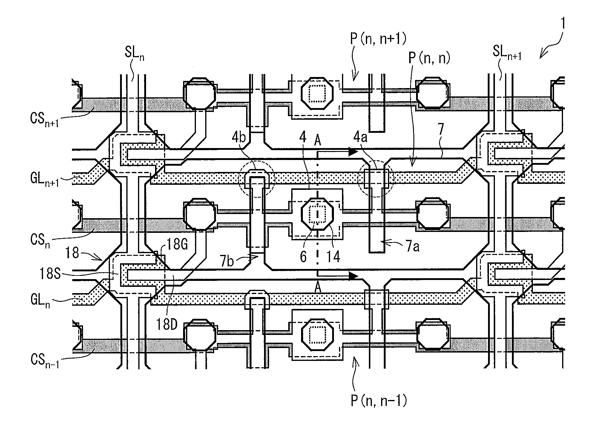
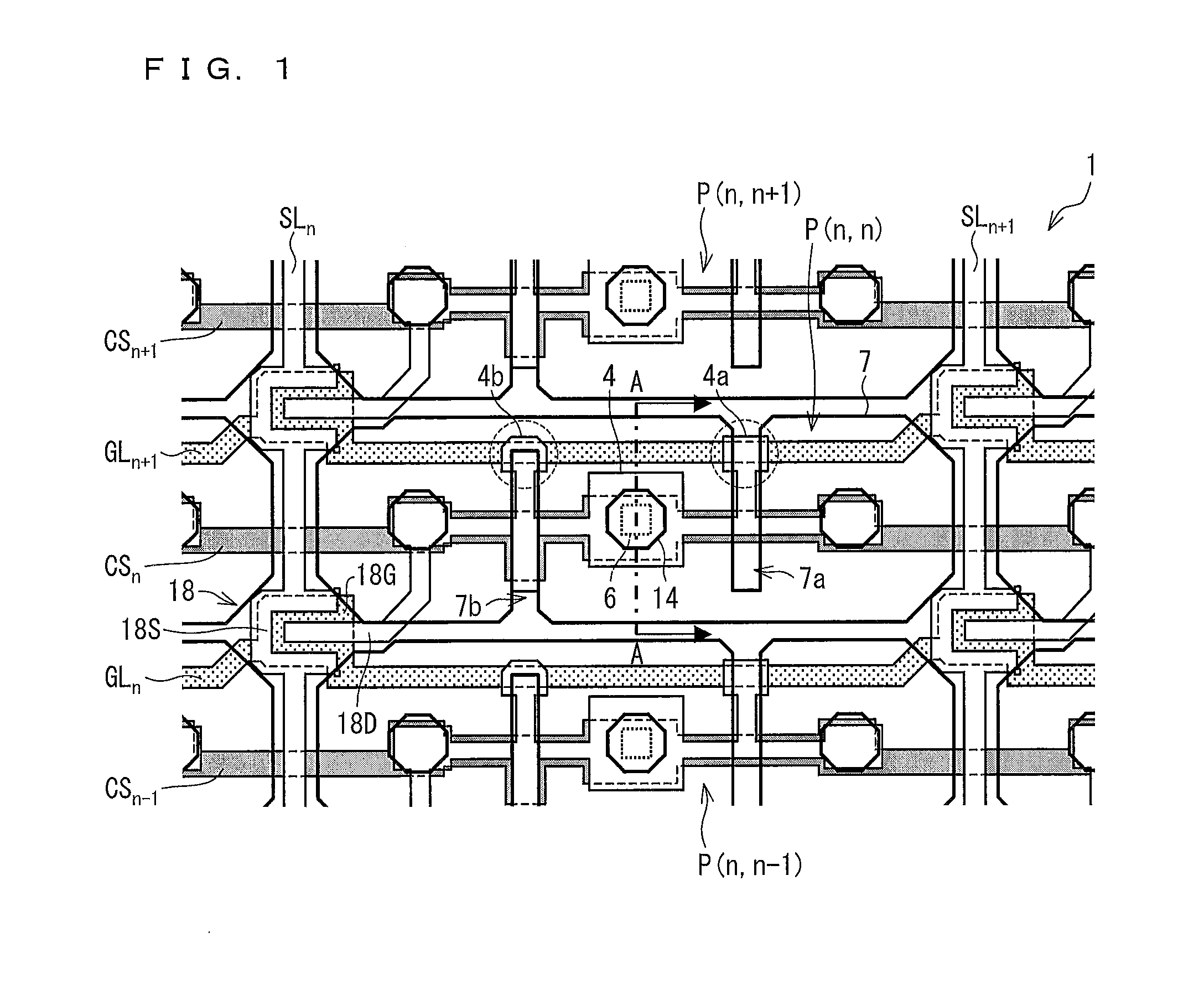
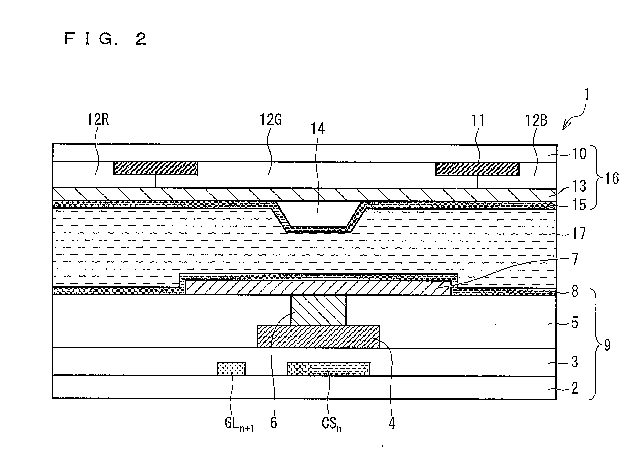
[0056]The following description will discuss Embodiment 1 of the present invention, with reference to FIGS. 1 through 3.

[0057]Embodiment 1 will describe a VA (Vertical Alignment) mode liquid crystal display panel whose picture element electrode configuration has a CPA (Continuous Pinwheel Alignment) configuration. Note, however, that the present invention is not limited to this. The present invention can be applied, provided that (i) a scanning signal line is not completely covered with a picture element electrode (or sub-picture-element electrodes) in each picture element formation area and (ii) the scanning signal line, which is not covered with the picture element electrode, exists in each picture element. Examples of the picture element electrode to which the present invention is applicable encompass (i) a picture element electrode having an MVA (Multidomain Vertical Alignment) mode slits, (ii) an IPS (In Plane Switching) mode comb-teeth picture element electrode, (iii) a TBA (T...

embodiment 2

[0114]The following description will discuss Embodiment 2 of the present invention, with reference to FIGS. 4, 5, and 13. Embodiment 2 is different from Embodiment 1 in that a shield electrode 4c is extended from one of storage capacitor counter lines 4 of picture elements adjacent to each other in a direction in which data signal lines SL (SLn, SLn+1, and so forth) extend. The other configurations of Embodiment 2 are identical with those of Embodiment 1. For convenience, identical reference numerals are given to constituent members having functions identical with those of the constituent members illustrated in the drawings of Embodiment 1, and descriptions of such constituent members are omitted here.

[0115]FIG. 4 is a plane view illustrating a schematic shape of a picture element section in a liquid crystal display panel 1b of Embodiment 2.

[0116]Note that, also in FIG. 4, each picture element electrode 7 is not depicted in view of a stacking pattern of constituent members.

[0117]Acc...

embodiment 3

[0130]The following description will discuss Embodiment 3 of the present invention, with reference to FIGS. 6 and 7. Embodiment 3 is different from Embodiments 1 and 2 in that (i) each of scanning signal lines GL (GLn, GLn+1, and so forth) is bent so that the scanning signal line GL and at least one of notch parts 7a and 7b of each picture element electrode 7 do not overlap each other when viewed from above and (ii) a shield electrode 4d and a part of a scanning signal line GL, which part is located at a boundary between two picture elements, at least partially overlap each other when viewed from above. Note that (i) the two picture elements are adjacent to each other in a direction in which data signal lines SL (SLn, SLn+1, and so forth) extend and (ii) the shield electrode 4d is formed by extending a storage capacitor counter line 4 of one of the two picture elements. The other configurations of Embodiment 3 are identical with those of Embodiment 1. For convenience, identical refe...


PUM


Abstract

Picture element electrodes (7) are electrically connected with drain electrodes (18D) of respective transistor elements (18). The picture element electrodes (7) and data signal lines (SLn, SLn+1, . . . ) are provided above scanning signal lines (GLn, GLn+1, . . . ). The picture element electrodes (7) overlap scanning signal lines (GLn, GLn+1, . . . ) when viewed from above. Notch parts 7a and 7b are provided in each picture element electrode (7) so as to overlap each of the scanning signal lines (GLn, GLn+1, . . . ). Shield electrodes (4a, 4b) are formed in the same layer as the data signal lines (SLn, SLn+1, . . . ). Each of the scanning signal lines (GLn, GLn+1, . . . ) at least partially overlaps the shield electrodes (4a, 4b) in the notch parts (7a, 7b), when viewed from above. This provides the liquid crystal display panel having wide viewing angle characteristic and carrying out high quality display.

Description

TECHNICAL FIELD[0001]The present invention relates to a liquid crystal display panel and a liquid crystal display device. In particular, the present invention relates to a liquid crystal display panel and a liquid crystal display device in which one (1) picture element is divided into a plurality of domains such that liquid crystal molecules can be oriented in multiple directions.BACKGROUND ART[0002]In recent years, liquid crystal display devices are rapidly becoming popular as alternatives to cathode-ray tubes (CRTs). Such liquid crystal display devices are used in a wide variety of devices, such as television devices, monitors, and mobile phones, because of their characteristics such as energy saving, reduced thickness, and lightweight.[0003]In particular, there has been recently grown the so-called mobile device equipped with (i) a battery functioning as a power supply and having limited capacity and (ii) a liquid crystal display device functioning as display means.[0004]In such ...

Claims


Application Information

Patent Timeline
Patent Type & Authority Applications(United States)
IPC IPC(8): G09G3/36G06F3/038
CPCG02F1/136209G02F2001/136218G02F2201/123G02F1/136286G02F1/136218
Inventor ITOH, RYOHKIHISADA, YUHKOHORIUCHI, SATOSHIYAMADA, TAKAHARUYOSHIDA, MASAHIRO
Owner UNIFIED INNOVATIVE TECH
Why Eureka
Try Eureka