Terahertz interaction circuit

a technology of interaction circuit and terahertz wave, applied in the field of terahertz interaction circuit, can solve the problems of few developments in the field of terahertz oscillator or amplifier for generating terahertz waves

Active Publication Date: 2013-02-28
SAMSUNG ELECTRONICS CO LTD
View PDF6 Cites 16 Cited by
  • Summary
  • Abstract
  • Description
  • Claims
  • Application Information

AI Technical Summary

Benefits of technology

[0008]One of more embodiments provide a terahertz inte

Problems solved by technology

However, there have been few developments in the field of terahertz oscillators or a

Method used


Image

  • Terahertz interaction circuit
  • Terahertz interaction circuit
  • Terahertz interaction circuit

Examples


Embodiment Construction

[0038]Reference will now be made in detail to embodiments, examples of which are illustrated in the accompanying drawings, wherein like reference numerals refer to the like elements throughout. In this regard, the present embodiments may have different forms and should not be construed as being limited to the descriptions set forth herein. Accordingly, the embodiments are merely described below, by referring to the figures, to explain aspects of the present description.

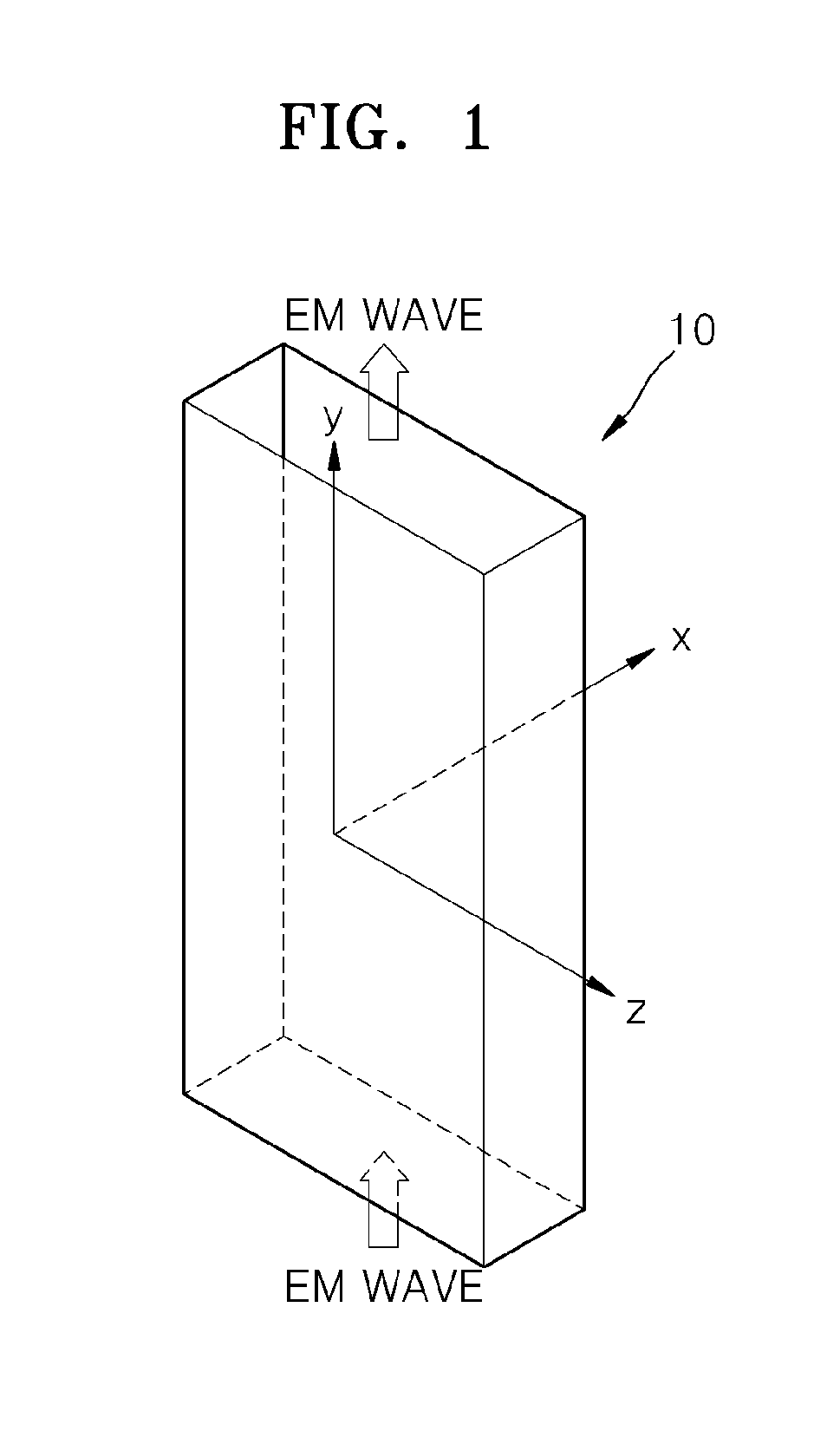
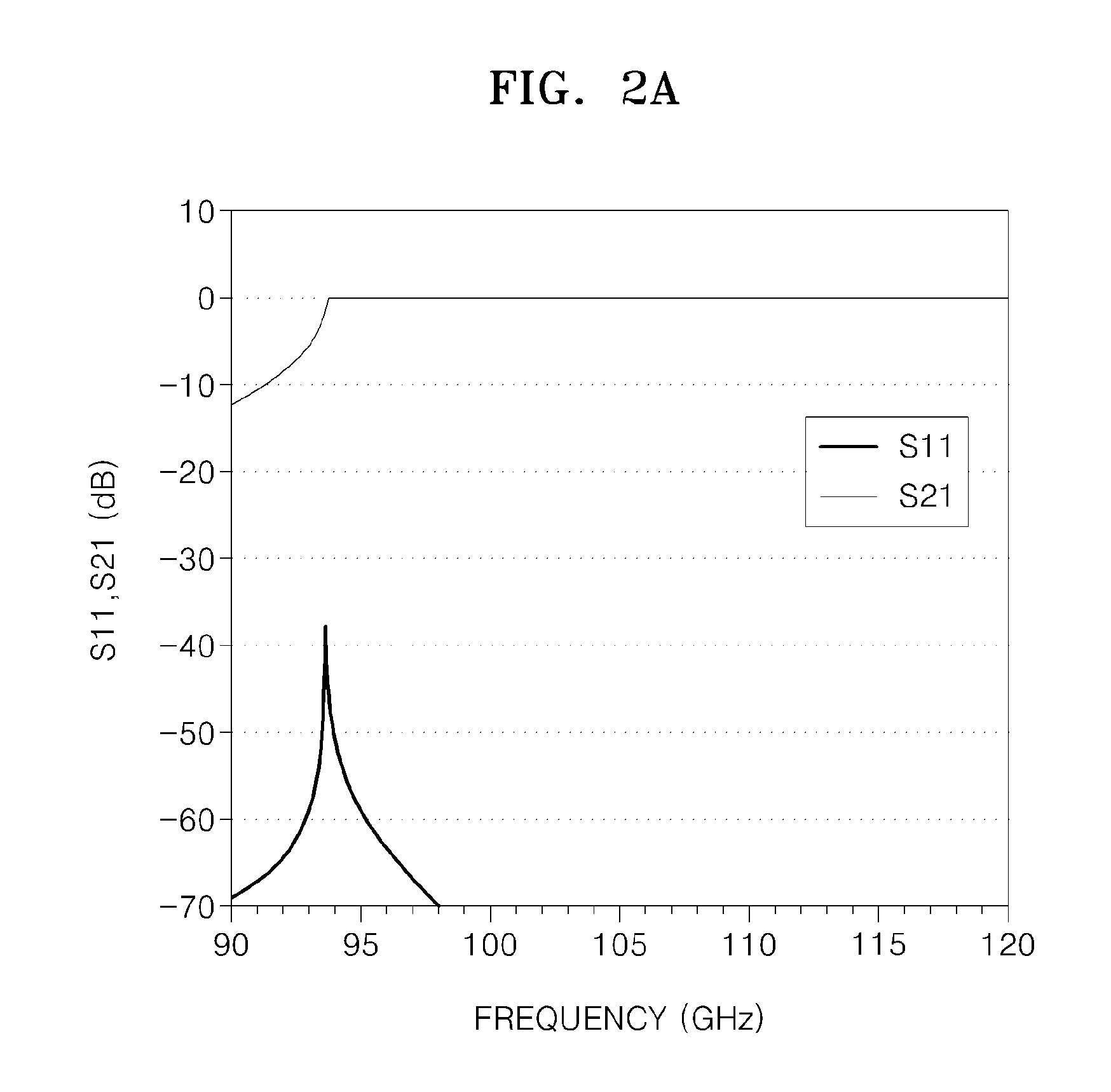
[0039]FIG. 1 illustrates a waveguide 10 having a uniform rectangular sectional shape. FIGS. 2A-2C illustrate results of a simulation calculated when a 100 GHz electromagnetic (EM) wave having a 1 W output is incident on the inside of the waveguide 10 of FIG. 1. In detail, FIG. 2a shows a result of a simulation of an s-parameter according to a frequency. FIG. 2B shows a result of a simulation of calculating Magnitude E and Complex Magnitude E in y direction. In FIG. 2B, Mag E indicates the magnitude of an electric fiel...


PUM


Abstract

A terahertz interaction circuit includes a waveguide through which electromagnetic waves pass, the waveguide having a folded shape and including a narrow open cavity portion; and an electron beam tunnel through which an electron beam passes, the electron beam tunnel penetrating through the waveguide.

Description

CROSS-REFERENCE TO RELATED APPLICATIONS[0001]This application claims priority from Korean Patent Application No. 10-2011-0084060, filed on Aug. 23, 2011, in the Korean Intellectual Property Office, the disclosure of which is incorporated by reference herein in it entirety.BACKGROUND[0002]1. Field[0003]The present disclosure relates to a terahertz interaction circuit, and more particularly, to a terahertz interaction circuit having a narrow open cavity structure.[0004]2. Description of the Related Art[0005]A terahertz frequency range between a microwave frequency range and an optical frequency range is used in the fields of molecular optics, biophysics, medical science, spectroscopy, or imaging or security. However, there have been few developments in the field of terahertz oscillators or amplifiers for generating terahertz waves due to physical and engineering limitations. Recently, as various new theories and fine processing technologies are introduced, the terahertz oscillators or...

Claims


Application Information

Patent Timeline
IPC IPC(8): G02B6/12
CPCG01N21/3581G02B6/12H01S1/00
Inventor BAIK, CHAN-WOOKAHN, HO-YOUNG
Owner SAMSUNG ELECTRONICS CO LTD
Why Eureka
Try Eureka