Integrated Backscattered Electron Detector with Cathodoluminescence Collection Optics

an electron detector and optics technology, applied in the field of image detectors for electron microscopy, can solve the problems of obscuring the signal to the back scattering electron detector, compromising the solid angle subtended by the back scattering detector in comparison to normal operation, and compromising the use of other detectors at the same tim

Active Publication Date: 2013-04-25
GATAN INC
View PDF0 Cites 5 Cited by
  • Summary
  • Abstract
  • Description
  • Claims
  • Application Information

AI Technical Summary

Problems solved by technology

Where the optical element used to direct the emitted photons covers such a large solid angle the use of other detectors simultaneously is compromised unless line of sight is provided by sacrificing the solid angle subtended by the optical element.
1) The emission direction of backscattered electrons and photons is similar and therefore collectors / detectors are required to occupy the same space. Therefore, a large sacrifice in both signals is required so that they may be sensed simultaneously. Backscattered electron detectors are typically mounted to the bottom of the pole piece or inserted immediately below, and the optical element used to direct photons is typically situated between the sample and the backscattered detector, thus obscuring the signal to the back scattered electron detector.
2) Sacrificing part of the optical element's solid angle allows the backscattered detector line of sight to the sample, however the optical element is typically thick (4-20 mm) and the distance between the sample and the backscattered detector large therefore further compromising the solid angle subtended by the backscattered detector in comparison to normal operation.
Detection of photons and backscattered electrons simultaneously is not novel; however, this has only been achieved through large sacrifices in efficiency—typically greater than or equal to 50% reduction in comparison to optimum operation of either detector.
This is often unacceptable for many applications.
Furthermore, this has only been achieved by the use of two separate instruments.

Method used


Image

  • Integrated Backscattered Electron Detector with Cathodoluminescence Collection Optics
  • Integrated Backscattered Electron Detector with Cathodoluminescence Collection Optics
  • Integrated Backscattered Electron Detector with Cathodoluminescence Collection Optics

Examples


Embodiment Construction

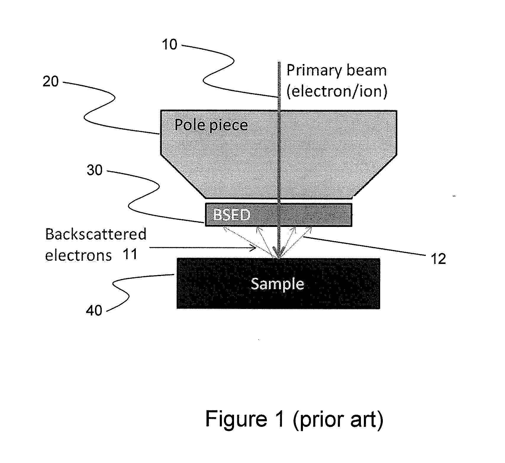
[0017]FIG. 1 shows a standard electron microscope with a direct detection backscattered electron detector 30. The electron beam 10 is directed through the pole piece 20 and the detector 30 to the sample 40. Backscattered electrons 11 leave the surface of the sample 20 and are detected by the detector 30. The detector is a direct electron detector as opposed to a detector comprising a scintillator that converts electrons to photons.

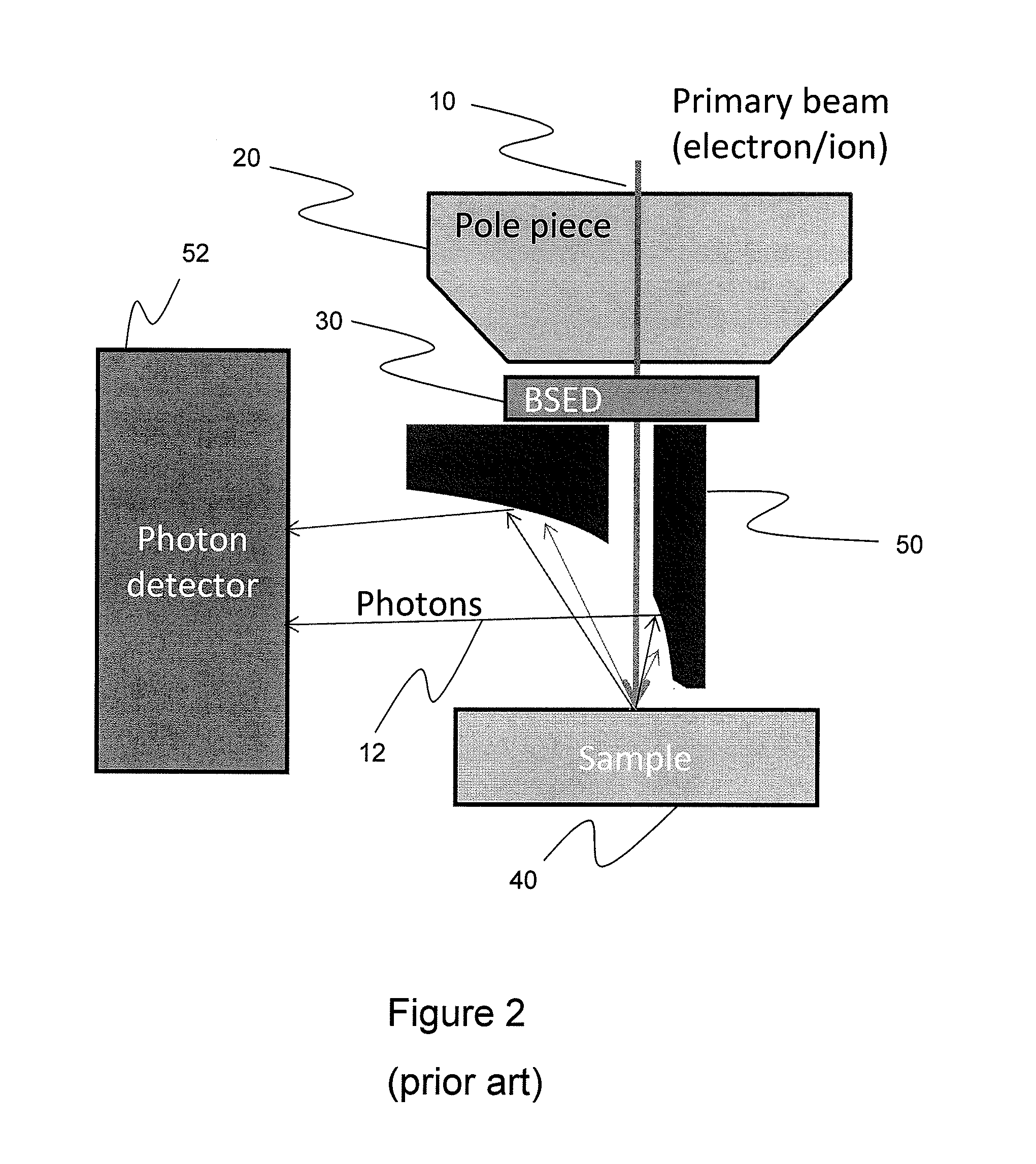
[0018]FIG. 2 shows a prior art system for detecting cathodoluminescence photons 14 produced in the sample 40. A photon collection mirror 50 is placed between the backscattered electron detector 30 and the sample 40. Photons 12 produced by the sample 40 are directed by the mirror 50 to a photon detector 52. This configuration has the disadvantage that the mirror blocks a significant portion of the backscattered electrons from reaching the detector 30.

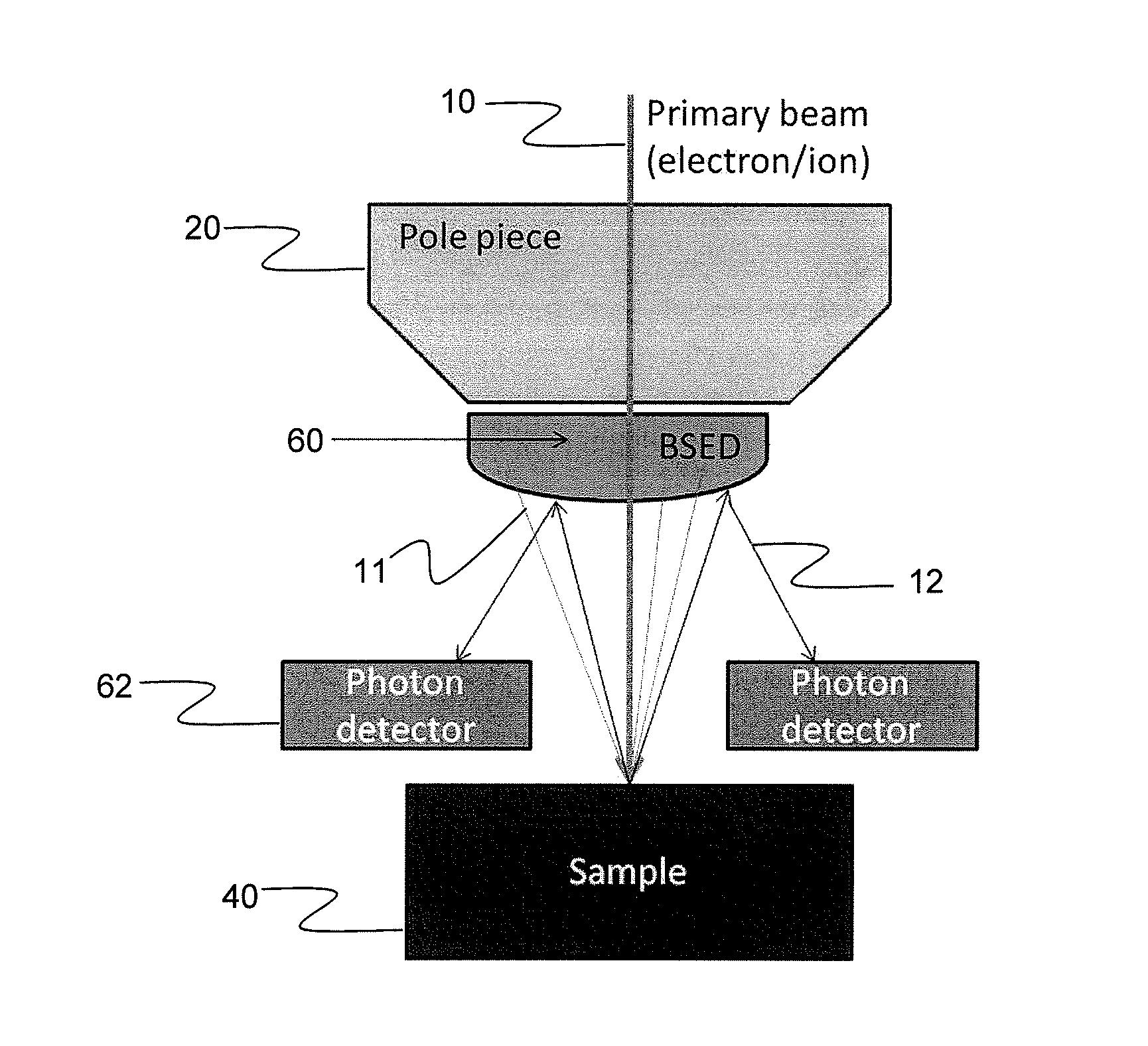
[0019]In an embodiment of the invention shown in FIG. 3, a semiconductor diode 60 for sensing backscattered ...


PUM


Abstract

An apparatus for simultaneous detection of backscattered electrons and photons from a sample. The device includes a direct detection backscattered electron detector and a photon detector. The backscattered electron detector has a reflective surface that reflects photons emitted by the sample onto the photon detector.

Description

FIELD OF THE INVENTION[0001]This invention relates to image detectors for electron microscopy. In particular the invention relates to simultaneous detection of backscattered electrons and cathodoluminescence emitted by a sample.BACKGROUND OF THE INVENTION[0002]When a high energy electron or ion beam strikes a sample, photons can be emitted. These emitted photons are also known as cathodoluminescence. The collection and detection of these photons in the wavelength range from UV through visible to IR, can provide a wealth of information about the sample under investigation. However, the signal to be detected can be small and in order to obtain the highest signal to noise ratio, minimize acquisition times and reduce the excitation energy required it is desirable to collect the largest proportion of emitted photons as possible. The most efficient manner of collecting photons emitted from a sample in an electron microscope is by using an optical element which subtends a large solid angle...

Claims


Application Information

Patent Timeline
Patent Type & Authority Applications(United States)
IPC IPC(8): H01J37/26
CPCH01J37/244H01J2237/24475H01J2237/2445H01J2237/2441
Inventor STOWE, DAVID J.HUNT, JOHNGALLOWAY, SIMON A.
Owner GATAN INC
Why Eureka
Try Eureka