
Efficient Polarization Independent Single Photon Detector

a single photon detector and polarization independent technology, applied in the direction of optical radiation measurement, pulse technique, instruments, etc., can solve the problems of reducing the quantum efficiency of sn-spd's, difficult to create nanowires, and channel features smaller than 100 nanometers, so as to achieve the effect of signal-to-noise and quantum efficiency. high

Active Publication Date: 2014-03-27
GOVERNMENT OF THE UNITED STATES OF AMERICA AS REPRESENTED BY THE SEC OF COMMERCE THE NAT INST OF STANDARDS & TEHCNOLOGY
View PDF4 Cites 34 Cited by
  • Summary
  • Abstract
  • Description
  • Claims
  • Application Information

AI Technical Summary

Benefits of technology

The invention is a new kind of detector that can detect single photons with higher efficiency and accuracy than other detectors. It is made using a special material called a polarization independent superconducting nanowire. This makes it easier to use and more reliable for detecting small amounts of light.

Problems solved by technology

Another problem known in the art is that the quantum efficiency of SN-SPD's degrades as the width of the nanowires increase, and therefore microelectronic circuits in the prior art have been limited to the use of extremely narrow nanowires.
Current electron beam fabrication methods make it extremely difficult to create nanowires and channel features smaller than 100 nanometers.
A limiting factor governing the quantum efficiency of SN-SPD microelectronic circuits based on NbN is that they have a relatively small area where absorption of photons may take place.
Another problem known in the art is that SPD devices experience decreased quantum efficiencies for photons having longer wave lengths.
Another problem known in the art is that the detection efficiency of SNSPD's depends upon the polarization of the light.

Method used


Image

  • Efficient Polarization Independent Single Photon Detector
  • Efficient Polarization Independent Single Photon Detector
  • Efficient Polarization Independent Single Photon Detector

Examples


Embodiment Construction

[0038]For the purpose of promoting an understanding of the present invention, references are made in the text to exemplary embodiments of a single photon detector with optimized reactive surface geometry only some of which are described herein. It should be understood that no limitations on the scope of the invention are intended by describing these exemplary embodiments. One of ordinary skill in the art will readily appreciate that alternate but functionally equivalent components may be used. The inclusion of additional elements may be deemed readily apparent and obvious to one of ordinary skill in the art. Specific elements disclosed herein are not to be interpreted as limiting, but rather as a basis for the claims and as a representative basis for teaching one of ordinary skill in the art to employ the present invention.

[0039]It should be understood that the drawings are not necessarily to scale; instead emphasis has been placed upon illustrating the principles of the invention. ...


PUM

PropertyMeasurementUnit
photon wavelengthaaaaaaaaaa

Abstract

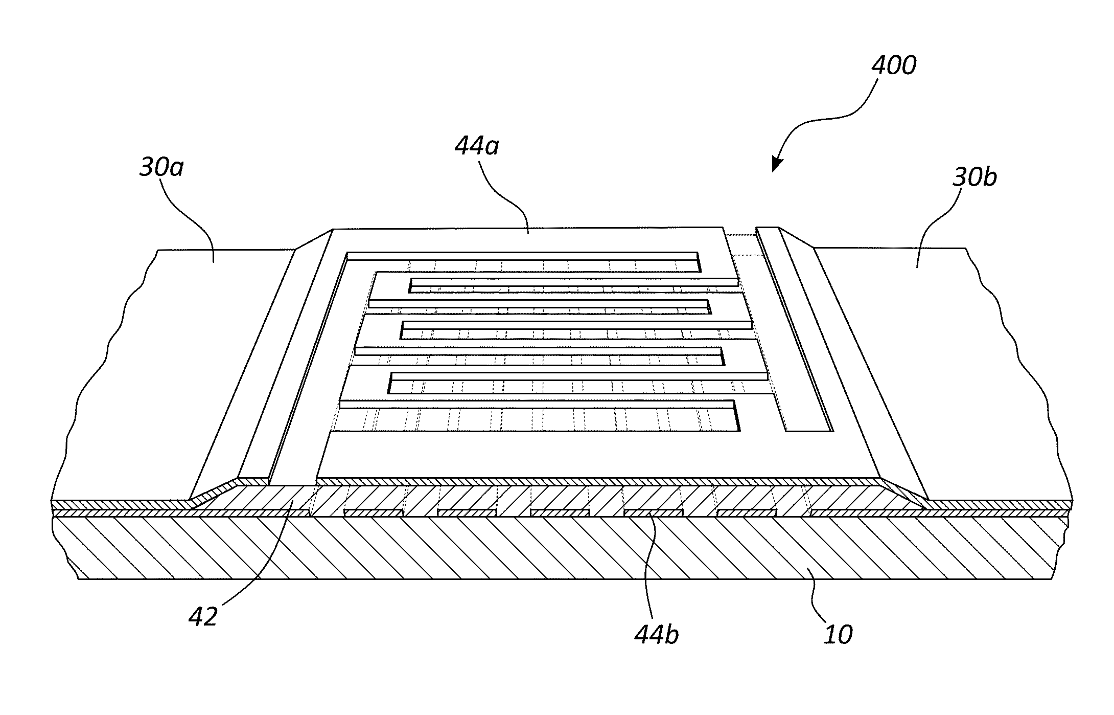
A superconducting nanowire single photon detector (SN-SPD) microelectronic circuit is described which has higher quantum efficiency and signal-to-noise than any SN-SPD's known in the art. The material and configuration of the microelectronic circuit eliminates the polarization dependence and shows improved signal-to-noise over SN-SPD microelectronic circuits known in the art. The higher efficiency, polarization independence, and high signal-to-noise is achieved by vertically stacking two tungsten-silicide (TS) SN-SPDs and electrically connecting them in parallel. This structure forms a multilayer superconducting nanowire avalanche photo-detector (SNAP). A single photon detection device employing the multilayer (SNAP) microelectronic circuit demonstrates a peak system detection efficiency of 87.7% and a polarization dependence of less than 2%. This represents nearly an order of magnitude improvement in both system detection efficiency and reduction of polarization dependence compared to conventional SNSPDs.

Description

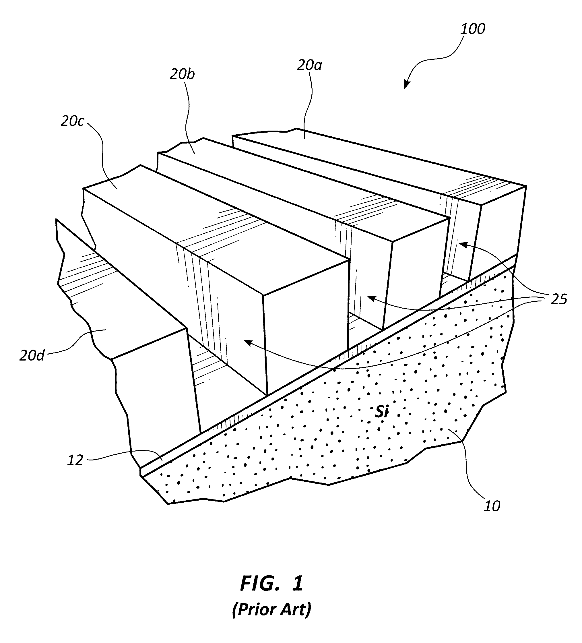
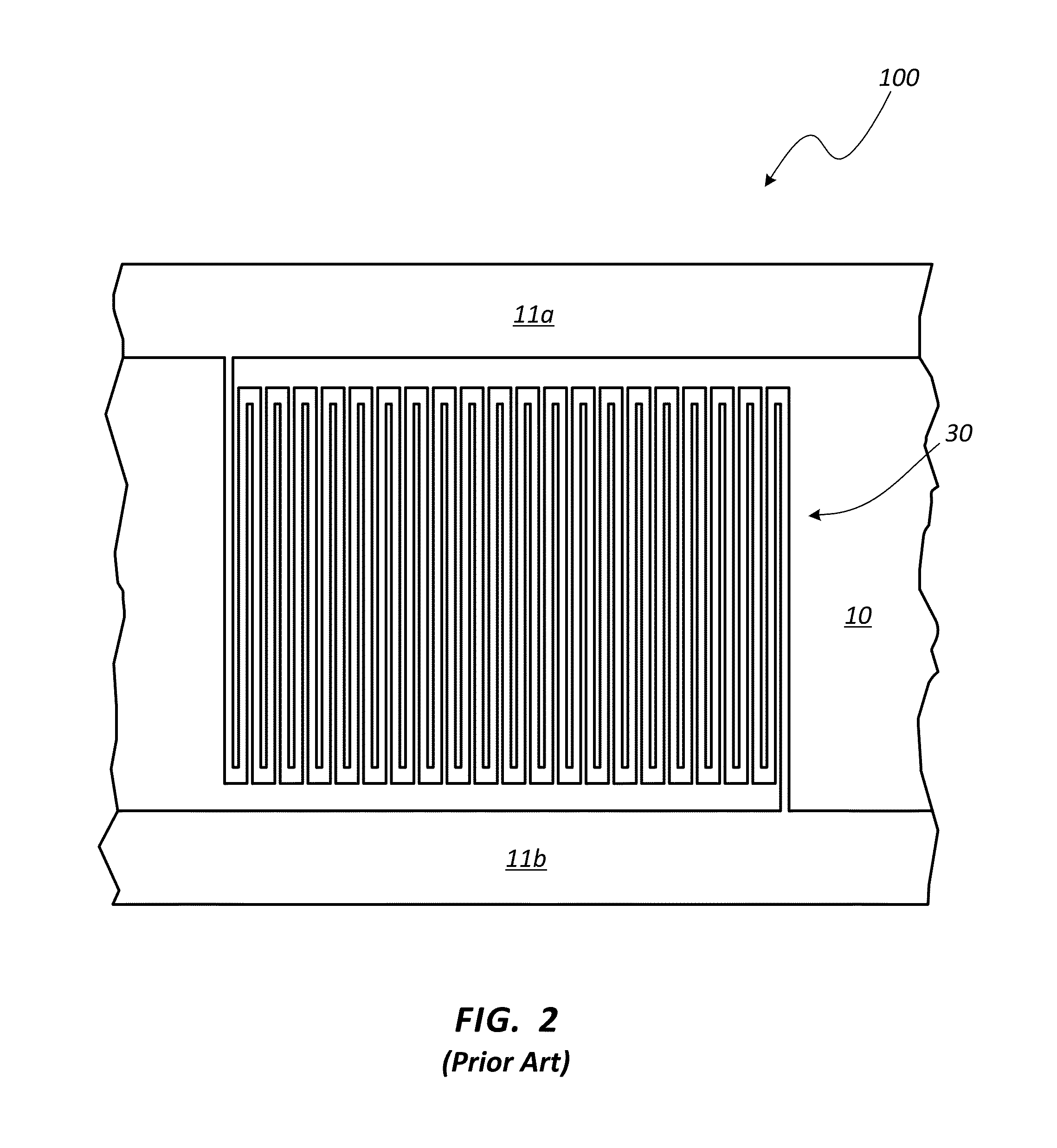
CROSS-REFERENCE TO RELATED APPLICATIONS[0001]This application claims priority to U.S. Provisional Application No. 61 / 638,675 filed on Apr. 26, 2012.STATEMENT OF GOVERNMENT INTEREST[0002]The invention described herein was made by employees of the United States Government and may be manufactured and used by or for the Government of the United States of America for governmental purposes without the payment of any royalties thereon or therefor.FIELD OF THE INVENTION[0003]The present invention relates to the field of single photon detectors, and more specifically to a photon detector which more efficiently detects photons in low light environments.BRIEF DESCRIPTION OF THE DRAWINGS[0004]The patent or application file contains at least one drawing executed in color. Copies of this patent or patent application publication with color drawing(s) will be provided by the Office upon request and payment of the necessary fee.[0005]FIG. 1 is a cut-away perspective of an exemplary single layer supe...

Claims


Application Information

Patent Timeline
Patent Type & Authority Applications(United States)
IPC IPC(8): H01L39/02H01L39/24
CPCH01L39/24H01L39/02G01J1/42G01J2001/442G01J1/0425H10N60/84H10N60/85H10N60/01H10N60/80
Inventor NAM, SAE WOOBAEK, BURM
Owner GOVERNMENT OF THE UNITED STATES OF AMERICA AS REPRESENTED BY THE SEC OF COMMERCE THE NAT INST OF STANDARDS & TEHCNOLOGY
Learn More