Three-dimensional island pixel photo-sensor

a three-dimensional island and photo-sensor technology, applied in the field of three-dimensional island pixel photo-sensors, can solve the problems of p-n diodes degrading further, cmos image sensors have relatively poor pixel density, and higher current flow in the external circui

Inactive Publication Date: 2004-04-13
IBM CORP
View PDF6 Cites 54 Cited by
  • Summary
  • Abstract
  • Description
  • Claims
  • Application Information

AI Technical Summary

Benefits of technology

The light absorption sidewall regions are perpendicular to the surface of the pixel that receives the incident light, while conventional light absorption regions are made parallel to the pixel surface. With the invention, the upper surface of the island maintains the necessary logic circuitry and the upper surface is not a region where substantial amounts of light are absorbed. To the contrary, with the invention, the openings surrounding each pixel island allow angled light beams to directly strike the vertical light absorption surfaces. Further, light beams that are directly perpendicular to the upper surface of the array of are reflected from the trenches surrounding each of the islands to one of the adjacent vertical light absorption regions. Also, the light beams will produce multiple internal reflections inside the pixel island, which also improves the diode quantum efficiency.
Since the light absorption regions are perpendicular to the upper surface of the array, they do not consume any substantial amount of the two-dimensional area of the upper surface of the array. Only logic circuitry and the trenches between the pixel islands consume two-dimensional area of the upper surface of the array. Thus, the inventive three-dimensional photo-diode island design realizes an increase in sensor packing density.

Problems solved by technology

At long wavelengths, the required absorption depth becomes very long which causes performance of p-n diodes to degrade further.
This results in higher current flow in the external circuit than that of the p-n diode sensors due to large drift space.
Therefore, conventional CMOS image sensors have relatively poor pixel density and there is a need to increase the pixel density.
Only logic circuitry and the trenches between the pixel islands consume two-dimensional area of the upper surface of the array.

Method used


Image

  • Three-dimensional island pixel photo-sensor
  • Three-dimensional island pixel photo-sensor
  • Three-dimensional island pixel photo-sensor

Examples


Embodiment Construction

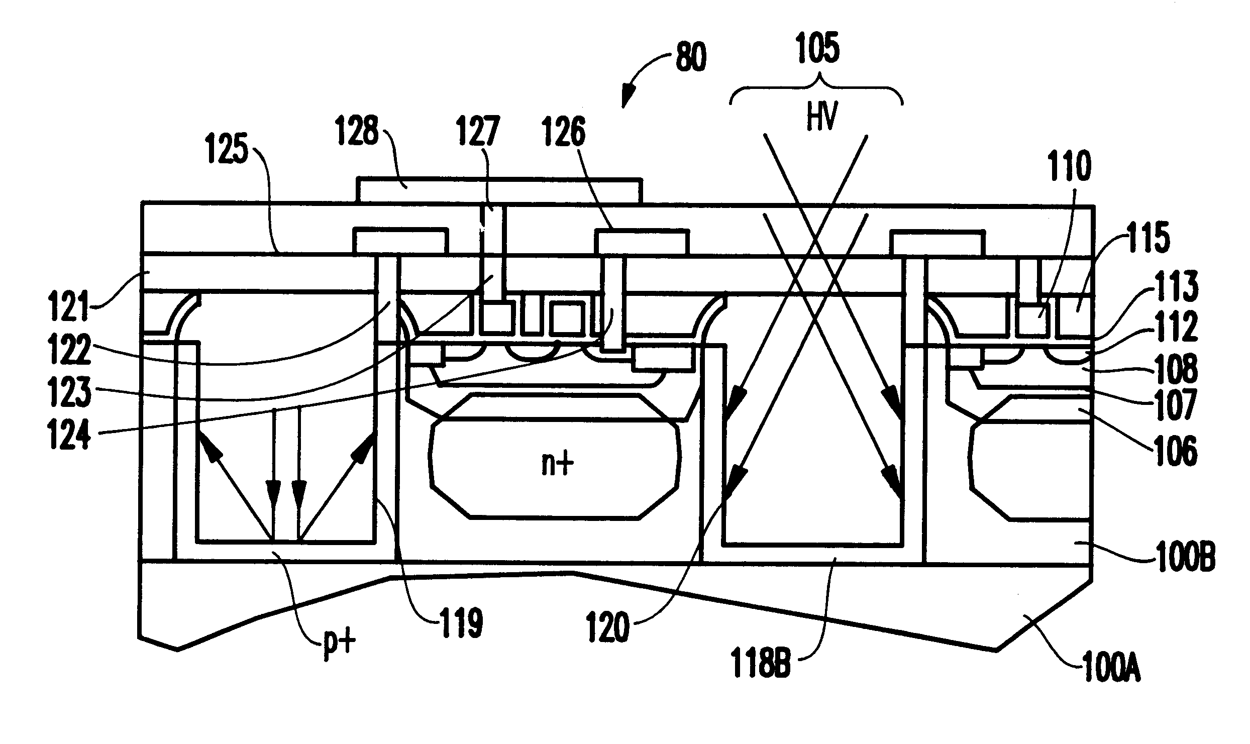
As shown above, there is a need to increase pixel density in image sensor arrays. The invention increases pixel density with a new photo-sensor pixel structure that has the p+ diffusion of the p-i-n diode formed at the outer edges of pixel islands. Correspondingly, the n+ of the p-i-n diode is formed in the core of the island, and the i layer is the middle ring formed between the outer edge of p+ layer and the n+ core. In the inventive structure, the light absorption regions are located along the vertical walls of the island (e.g, perpendicular to the upper surface of the array). By placing the light absorption regions along the vertical walls of the three-dimensional island, the area occupied by the light absorption regions is increased dramatically resulting in a substantial improvement in diode quantum efficiency.

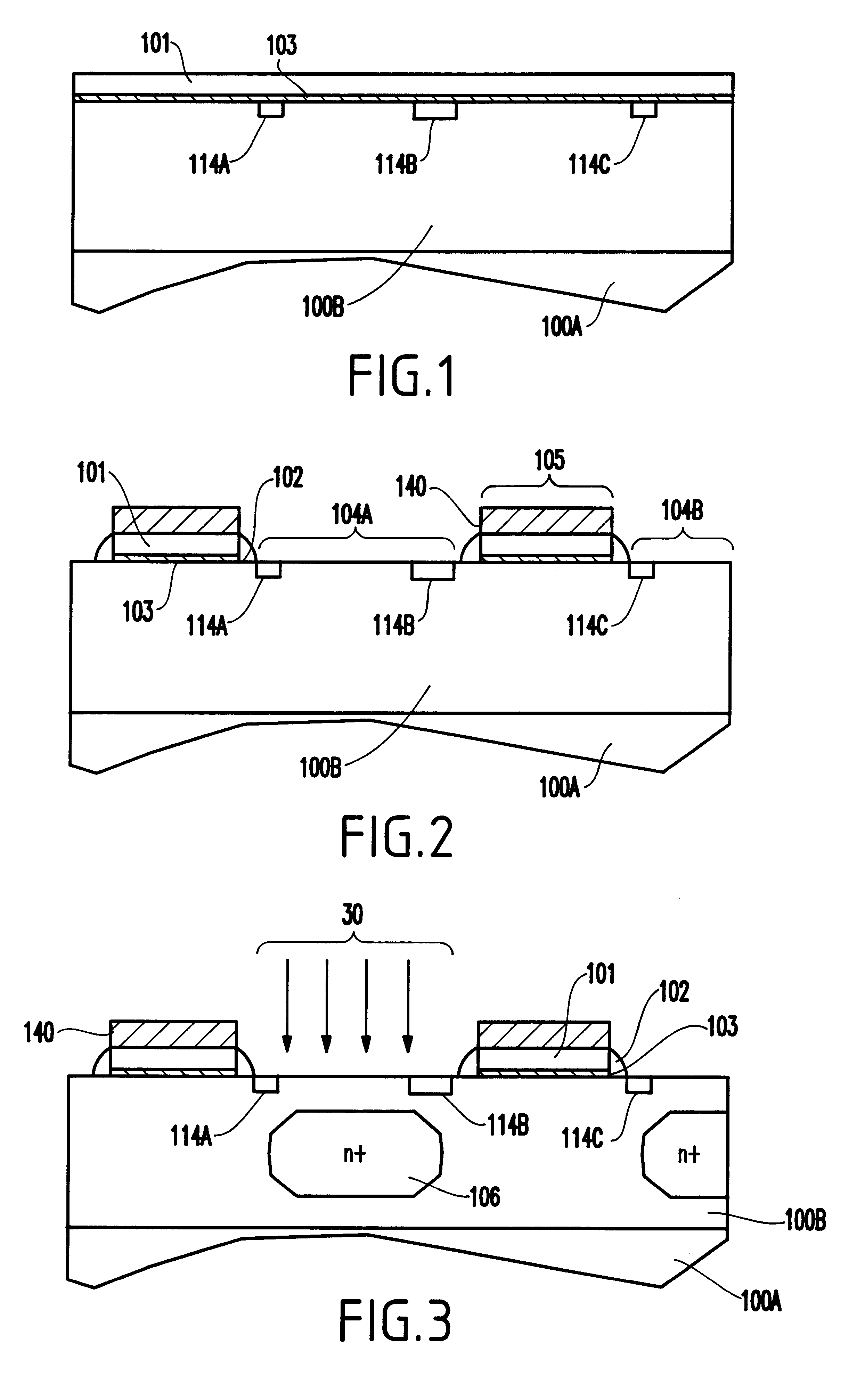
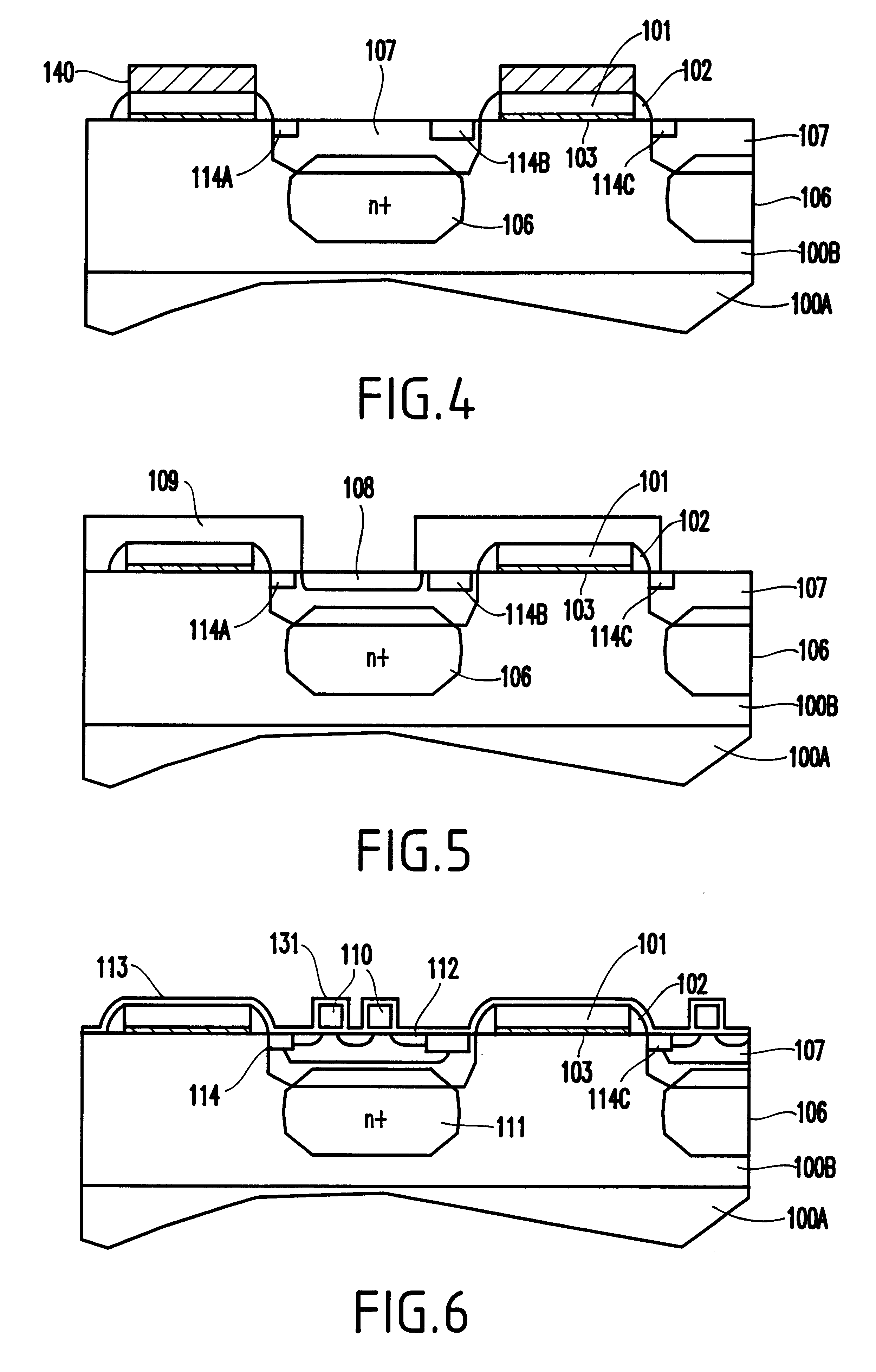
As shown in FIGS. 12 and 13A, that are discussed in greater detail below, the light absorption regions are perpendicular to the upper surface of the pixel (as opposed to...


PUM


Abstract

A method and structure for a photodiode array comprising a plurality of photodiode cores, light sensing sidewalls along an exterior of the cores, logic circuitry above the cores, trenches separating the cores, and a transparent material in the trenches is disclosed. With the invention, the sidewalls are perpendicular to the surface of the photodiode that receives incident light. The light sensing sidewalls comprise a junction region that causes electron transfer when struck with light. The sidewalls comprise four vertical sidewalls around each island core. The logic circuitry blocks light from the core so light is primarily only sensed by the sidewalls.

Description

1. Field of the InventionThe present invention generally relates to photo-sensor arrays and more particularly to a unique three-dimensional pixel structure that significantly improves pixel packing density.2. Description of the Related ArtSemiconductor photosensors have been found in a wide variety of applications. These include position measurement, CMOS imagine sensors, motion detector, image capturing and velocity measurement. One key application of these devices however is for optical-fiber communication.The basic photo sensing mechanisms, as summrarized by S. M. Sze in the text book of Physics of Semiconductor Devices, p. 743 (incorporated herein by reference), are: (1) carrier generation by incident light, (2) carrier transport and / or multiplication by some sort of current-gain devices, and (3) interaction of current and IC circuits to provide output signals. A well-designed photo-sensor provides high sensitivity at operating wavelengths, high response speed, and minimum noise...

Claims


Application Information

Patent Timeline
Patent Type & Authority Patents(United States)
IPC IPC(8): H01J40/00H01J40/14H01L29/06H01L31/06H01L29/02H01L31/00H01L31/062H01L27/146
CPCH01L27/1463H01L27/14634H01L27/14643
Inventor CLEVENGER, LAWRENCE A.HSU, LOUIS L.RADENS, CARL J.WANG, LI-KONGWONG, KWONG HON
Owner IBM CORP
Why Eureka
Try Eureka