Structure for and method of fabricating a high-speed CMOS-compatible Ge-on-insulator photodetector

a technology of ge-on-insulator and photodetector, which is applied in the field of ge-on-insulator photodetector, can solve the problems of high-efficiency photodetector, device difficulty in achieving high speed, and inability to collect carriers, and achieve high quantum efficiency, low voltage operation, and high bandwidth

Active Publication Date: 2006-11-21
GLOBALFOUNDRIES US INC
View PDF7 Cites 55 Cited by
  • Summary
  • Abstract
  • Description
  • Claims
  • Application Information

AI Technical Summary

Benefits of technology

[0009]Advantageously, the photodetectors of the present invention achieve: (a) high bandwidth by utilizing a buried insulating layer to isolate carriers generated in the underlying substrate, (b) high quantum efficiency over a broad spectrum by utilizing a Ge absorbing layer, (c) low voltage operation by utilizing an absorbing layer that is thin and narrow electrode spacings, and (d) compatibility with CMOS devices by virtue of its planar structure and use of a Group IV absorbing material. Examples of Group IV absorbing materials include C, Si, Ge, Sn, Pb and combinations thereof.
[0010]The present invention also provides a method for fabricating a high-performance photodetector using direct growth of Ge on a thin SOI layer, and subsequent thermal annealing to achieve a high-quality absorbing layer.
[0011]Advantageously, the method of the present invention limits the amount of Si available for interdiffusion, thereby allowing the Ge layer to be annealed without causing substantial dilution of the Ge layer by the underlying Si.

Problems solved by technology

In the semiconductor industry, there has been a problem with creating a high-speed, high-efficiency photodetector that is compatible with conventional Si complementary metal oxide semiconductor (CMOS) technology.
Despite its ease of integration with CMOS, this device has problems achieving high speed because of RC delays due to its high capacitance, as well as limitations in its ability to collect carriers generated deeper than the trench depth.
547, 2001) can improve the latter problem somewhat, though, due to the depth of the fingers (several microns), these innovations are not easy to integrate into a standard CMOS process.
However, this technique has the problem that very thick layers (on the order of greater than 1 μm) are needed to reduce the dislocation density and also ensure that all the light is collected in the top Ge layer.
This can lead to reduced bandwidth because carriers generated deep within the substrate have a longer distance to reach the electrodes.
The thick layers also cause problems with integration because thick layers typically create a non-planar surface for processing.
However, this technique has the problem that for shorter wavelength light (such as, for example, 850 nm), carriers are also generated in the underlying Si layer, greatly reducing the speed of the detector.
Moreover, Ge grown directly on Si has a high defect density, and either selective-area growth or high-temperature annealing is needed to reduce the dislocation density.
The annealing is especially problematic, because it can lead to significant Si diffusion into the Ge layer, which can greatly reduce the absorption.
The interdiffusion is a particular problem for thin Ge layers, as the Si can diffuse throughout the entire Ge layer.
However, this technique has the problem that it only has high absorption near the resonance wavelength, which can be a fairly narrow peak.
Also, fabrication of the bottom mirror and the lateral overgrowth epitaxy required to produce Si over this mirror is complicated.
However, the '828 patent does not describe a specific structure that could actually achieve high performance or be CMOS compatible, nor does it provide a method by which such a structure could be made.

Method used


Image

  • Structure for and method of fabricating a high-speed CMOS-compatible Ge-on-insulator photodetector
  • Structure for and method of fabricating a high-speed CMOS-compatible Ge-on-insulator photodetector
  • Structure for and method of fabricating a high-speed CMOS-compatible Ge-on-insulator photodetector

Examples


Embodiment Construction

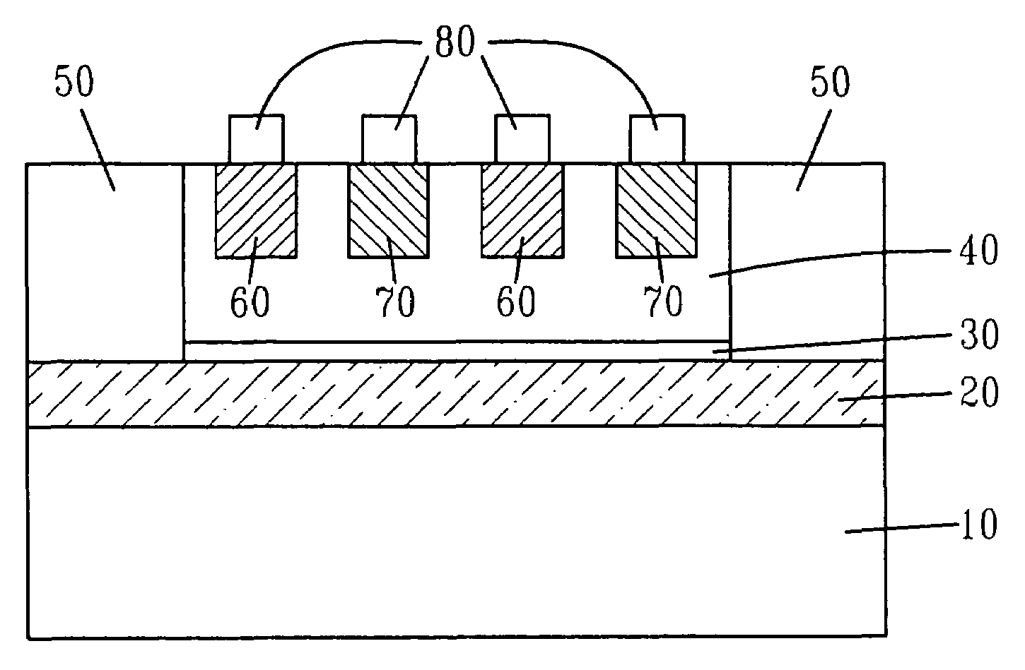
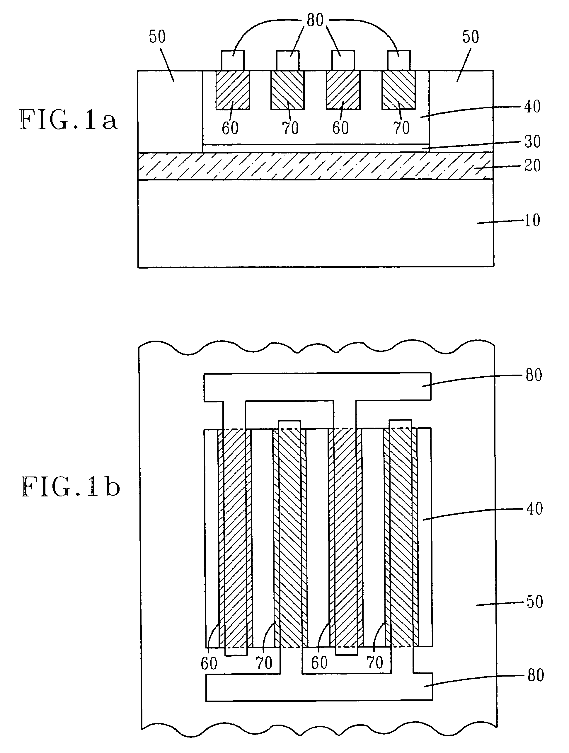
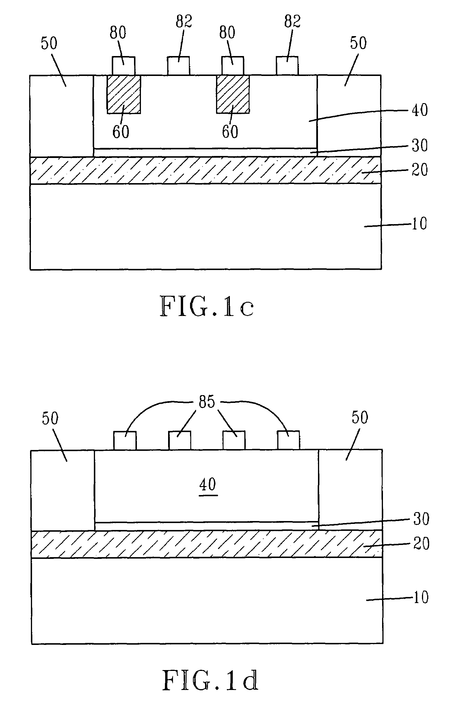
[0023]Cross-sectional and plan-view diagrams of one embodiment of the present invention are shown in FIGS. 1(a) and 1(b). As shown in FIG. 1(a), the present invention provides a Ge-on-insulator photodetector that is composed of a single-crystal semiconductor substrate 10 (e.g., Si, Ge, SiGe, GaAs, InAs, SiGeC or SiC), an insulating layer 20 (e.g., an oxide, nitride, oxynitride or any combination thereof), and a thin layer of essentially Si (hereinafter Si layer) 30 (e.g., an SOI layer, epi-Si, or amorphous Si). In a preferred embodiment of the present invention, the initial substrate is a Si-on-insulator (SOI) wafer, and therefore layer 10 is Si, and layer 20 is a buried oxide, e.g., SiO2. On top of the thin Si layer 30, is a layer of essentially Ge (hereinafter Ge layer) 40 which, in accordance with the present invention, is much thicker than the Si layer 30. In a preferred embodiment of the present invention, layers 30 and 40 are not-intentionally doped, and should have as low a d...


PUM


Abstract

The invention addresses the problem of creating a high-speed, high-efficiency photodetector that is compatible with Si CMOS technology. The structure consists of a Ge absorbing layer on a thin SOI substrate, and utilizes isolation regions, alternating n- and p-type contacts, and low-resistance surface electrodes. The device achieves high bandwidth by utilizing a buried insulating layer to isolate carriers generated in the underlying substrate, high quantum efficiency over a broad spectrum by utilizing a Ge absorbing layer, low voltage operation by utilizing thin a absorbing layer and narrow electrode spacings, and compatibility with CMOS devices by virtue of its planar structure and use of a group IV absorbing material. The method for fabricating the photodetector uses direct growth of Ge on thin SOI or an epitaxial oxide, and subsequent thermal annealing to achieve a high-quality absorbing layer. This method limits the amount of Si available for interdiffusion, thereby allowing the Ge layer to be annealed without causing substantial dilution of the Ge layer by the underlying Si.

Description

FIELD OF THE INVENTION [0001]The present invention relates to semiconductors and photodetectors and more particularly to germanium-on-insulator photodetectors and a method of fabricating the same.DESCRIPTION OF THE PRIOR ART [0002]In the semiconductor industry, there has been a problem with creating a high-speed, high-efficiency photodetector that is compatible with conventional Si complementary metal oxide semiconductor (CMOS) technology. As such, much research effort has been carried out in an attempt to solve this problem.[0003]One solution is the lateral trench detector described, for example, by M. Yang, et al., IEEE Elect. Dev. Lett., vol. 23, p. 395 (2002) and U.S. Pat. No. 6,177,289 to Crow, et al. This detector uses deep trenches in Si to collect light absorbed deep in the substrate. Despite its ease of integration with CMOS, this device has problems achieving high speed because of RC delays due to its high capacitance, as well as limitations in its ability to collect carri...

Claims


Application Information

Patent Timeline
Patent Type & Authority Patents(United States)
IPC IPC(8): H01L31/105H01L31/101
CPCH01L31/101Y02E10/548H01L31/10H01L31/00H01L27/146
Inventor CHU, JACK O.DEHLINGER, GABRIEL K.GRILL, ALFREDKOESTER, STEVEN J.OUYANG, QIGINGSCHAUB, JEREMY D.
Owner GLOBALFOUNDRIES US INC
Why Eureka
Try Eureka